
Loading article…
トランジスタ数は、電子デバイス(通常は単一の基板またはシリコンダイ上)内のトランジスタの数です。これは、集積回路の複雑さを測る最も一般的な指標です(ただし、現代のマイクロプロセッサ内のトランジスタの大部分は、同じメモリセル回路が何度も複製されたキャッシュメモリに含まれています)。MOSトランジスタ数の増加率は、一般的にムーアの法則に従います。ムーアの法則によれば、トランジスタ数は約2年ごとに倍増します。ただし、トランジスタ数はダイ面積に正比例するため、対応する製造技術の進歩度合いを表すものではありません。これをよりよく示すのは、半導体のトランジスタ数とダイ面積の比率であるトランジスタ密度です。
記録
2023年現在[update]、フラッシュメモリにおけるトランジスタ数が最も多いのは、5.3兆個のフローティングゲートMOSFET(トランジスタあたり3ビット)を搭載した、 Micronの2テラバイト(3Dスタック)16ダイ、232層V-NANDフラッシュメモリチップです。
2020年現在、シングルチッププロセッサのトランジスタ数が最も多いのは、CerebrasのディープラーニングプロセッサWafer Scale Engine 2[update]です。このプロセッサは、TSMCの7nm FinFETプロセスを使用して製造され、ウェハ上の84の露出フィールド(ダイ)に2.6兆個のMOSFETを備えています。 [1] [2] [3] [4] [5]
2024年現在[update]、トランジスタ数が最も多いGPUは、 TSMCのカスタム4NPプロセスノード上に構築され、合計2080億個のMOSFETを備えた NvidiaのBlackwellベースのB100アクセラレータです。
2023年6月現在、民生用マイクロプロセッサのトランジスタ数が最も多いのは、 TSMCの5nm半導体製造プロセスを使用して製造されたAppleのARMベースのデュアルダイM2 Ultra SoCの[update]1340億個のトランジスタです。[6]
多数の集積回路で構成されるコンピュータシステムに関して言えば、2016年時点でトランジスタ数が最も多いスーパーコンピュータ[update]は中国設計のSunway TaihuLightで、すべてのCPU/ノードを合わせると「ハードウェアの処理部に約400兆個のトランジスタ」があり、「DRAMには約12京個のトランジスタが含まれており、これはすべてのトランジスタの約97パーセントを占める」とのことです。[7]比較すると、2018年時点で米粒ほどの大きさしかない最小のコンピュータは[update]、トランジスタ数が約10万個でした。初期の実験的なソリッドステートコンピュータは、トランジスタ数がわずか130個でしたが、大量のダイオードロジックを使用していました。最初のカーボンナノチューブコンピュータは178個のトランジスタで、1ビット 1命令セットコンピュータでしたが、後継のコンピュータは16ビットです(ただし、命令セットは32ビットRISC-Vです)。
イオントランジスタチップ(「水ベース」アナログ限定プロセッサ)には、最大数百個のこのようなトランジスタが搭載されています。[8]
製造されたトランジスタの総数の推定値:
- 2014年まで:2.9 × 10 21
- 2018年まで:1.3 × 10 22 [9] [10]
トランジスタ数

マイクロプロセッサ
マイクロプロセッサは、コンピュータの中央処理装置の機能を単一の集積回路に組み込んだものです。これは、デジタル データを入力として受け取り、メモリに保存されている命令に従って処理し、結果を出力として提供する多目的のプログラム可能なデバイスです。
1960年代のMOS集積回路技術の発展は、最初のマイクロプロセッサの開発につながった。[11] 1970年に米海軍のF-14トムキャット戦闘機用にギャレットAIリサーチ社が開発した20ビットのMP944は、設計者のレイ・ホルトによって最初のマイクロプロセッサとみなされている。[12]これは6つのMOSチップで製造されたマルチチップマイクロプロセッサであった。しかし、1998年まで海軍によって機密扱いされていた。 1971年に発売された4ビットのIntel 4004は、最初のシングルチップマイクロプロセッサであった。
現代のマイクロプロセッサには通常、オンチップキャッシュメモリが搭載されています。これらのキャッシュメモリに使用されるトランジスタの数は、通常、マイクロプロセッサのロジックを実装するために使用されるトランジスタの数(つまり、キャッシュを除く)をはるかに上回ります。たとえば、最新のDEC Alphaチップでは、トランジスタの90%がキャッシュに使用されています。[13]
GPU
グラフィックス プロセッシング ユニット( GPU) は、メモリを迅速に操作および変更して、ディスプレイへの出力を目的としたフレーム バッファー内の画像の構築を高速化するように設計された特殊な電子回路です。
設計者とは、集積回路チップのロジックを設計するテクノロジー企業( NvidiaやAMDなど) を指します。製造元 (「Fab」) とは、ファウンドリで半導体製造プロセスを使用してチップを製造する半導体企業( TSMCやSamsung Semiconductorなど) を指します。チップ内のトランジスタ数は製造元の製造プロセスに依存し、半導体ノードが小さいほどトランジスタ密度が高くなり、トランジスタ数が多くなります。
GPUに付属するランダムアクセスメモリ( RAM)( VRAM、SGRAM、HBMなど)はトランジスタの総数を大幅に増加させ、通常、メモリはグラフィックカード内のトランジスタの大部分を占める。例えば、NvidiaのTesla P100には、 16GBのHBM2 メモリに加えて、GPU内に150億個のFinFET(16nm)があり、グラフィックカード上には合計約1500億個のMOSFETがある。 [194]次の表にはメモリは含まれていない。メモリのトランジスタ数については、以下のメモリのセクションを参照。
プログラマブルロジック
フィールドプログラマブル ゲート アレイ(FPGA) は、製造後に顧客または設計者が構成できるように設計された集積回路です。
メモリ
半導体メモリは電子データ記憶装置で、コンピュータメモリとしてよく使用され、集積回路上に実装されています。1970 年代以降のほぼすべての半導体メモリは、以前のバイポーラ接合トランジスタに代わってMOSFET (MOS トランジスタ)を使用しています。半導体メモリには、ランダム アクセス メモリ(RAM) と不揮発性メモリ(NVM) の 2 つの主要なタイプがあります。また、RAM にはダイナミック ランダム アクセス メモリ(DRAM) とスタティック ランダム アクセス メモリ(SRAM) の 2 つの主要なタイプがあり、NVM にはフラッシュ メモリと読み取り専用メモリ(ROM)の 2 つの主要なタイプがあります。
一般的なCMOS SRAM は、セルあたり 6 個のトランジスタで構成されています。DRAM の場合、1T1C (1 トランジスタと 1 コンデンサの構造) が一般的です。コンデンサの充電の有無 [ 要説明 ] によって1または0が保存されます。フラッシュ メモリでは、データはフローティング ゲートに保存され、トランジスタの抵抗が感知[要説明]されて保存されたデータが解釈されます。抵抗をどれだけ細かく分離できるか[要説明]に応じて、1 つのトランジスタに最大 3ビットを保存でき、トランジスタごとに 8 つの異なる抵抗レベルが可能になります。ただし、細かくすると再現性の問題が発生するため、信頼性が低下します。通常、フラッシュ ドライブには低グレードの 2 ビットMLC フラッシュが使用されるため、16 GB のフラッシュ ドライブには約 640 億個のトランジスタが含まれています。
SRAMチップでは、6トランジスタセル(1ビットあたり6つのトランジスタ)が標準でした。[293] 1970年代初頭のDRAMチップには3トランジスタセル(1ビットあたり3つのトランジスタ)がありましたが、1970年代半ばの4Kb DRAMの時代以降、シングルトランジスタセル(1ビットあたり1つのトランジスタ)が標準になりました。 [294] [295]シングルレベルフラッシュメモリでは、各セルに1つのフローティングゲートMOSFET (1ビットあたり1つのトランジスタ)が含まれますが、[296]マルチレベルフラッシュにはトランジスタあたり2、3、または4ビットが含まれます。
フラッシュメモリチップは一般的に層状に積み重ねられ、生産時には最大128層[297]、管理時には136層[298]まで積層され、メーカーからは最大69層のものがエンドユーザーデバイスに提供されています。
トランジスタコンピュータ
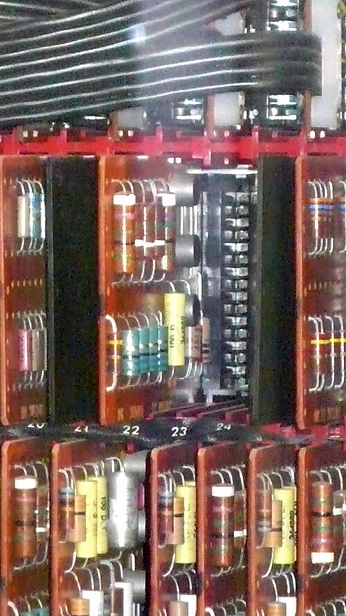
トランジスタが発明される前は、商用の集計機や初期の実験用コンピュータでリレーが使用されていました。世界で初めて機能したプログラム可能な全自動デジタルコンピュータ[357]は、1941年のZ3 22ビットワード長コンピュータで、2,600個のリレーを備え、約4~ 5Hzのクロック周波数で動作していました。1940年の複素数コンピュータのリレーは500個未満でしたが[358] 、完全にプログラム可能ではありませんでした。最も初期の実用的なコンピュータは、真空管と固体ダイオードロジックを使用していました。ENIACには18,000本の真空管、7,200本のクリスタルダイオード、1,500個のリレーがあり、真空管の多くには2つの三極管素子が含まれていました。
第二世代のコンピュータはトランジスタコンピュータであり、ディスクリートトランジスタ、ソリッドステートダイオード、磁気メモリコアで満たされた基板を特徴としていた。マンチェスター大学で開発された1953年の実験的な48ビット トランジスタコンピュータは、世界で初めて稼働したトランジスタコンピュータであると広く信じられている(プロトタイプには92個の点接触トランジスタと550個のダイオードがあった)。[359]後のバージョンである1955年のマシンには、合計250個の接合型トランジスタと1,300個の点接触ダイオードがあった。このコンピュータはクロックジェネレータに少数の真空管も使用していたため、完全にトランジスタ化された最初のコンピュータではなかった。1956年に電気技術研究所で開発されたETL Mark IIIは、プログラム格納方式を使用した最初のトランジスタベースの電子コンピュータであった可能性がある。これには「約130個の点接触トランジスタと約1,800個のゲルマニウムダイオードが論理素子として使用され、これらは300個のプラグインパッケージに収められており、差し込みおよび取り外しが可能であった。」[360] 1958年の10進アーキテクチャのIBM 7070は、完全にプログラム可能な最初のトランジスタコンピュータであった。約30,000個の合金接合ゲルマニウムトランジスタと22,000個のゲルマニウムダイオードが、約14,000枚の標準モジュラーシステム(SMS)カードに搭載されていた。1959年のMOBIDIC (「MOBIle DIgital Computer」の略)は、セミトレーラートラックのトレーラーに搭載された12,000ポンド(6.0ショートトン)の重量で、戦場データ用のトランジスタコンピュータであった。
第三世代のコンピュータは集積回路(IC)を使用した。[361] 1962年の15ビットの アポロ誘導コンピュータは、約12,000個のトランジスタと32,000個の抵抗器に対して「約4,000個の「タイプG」(3入力NORゲート)回路」を使用した。[362] 1964年に発表された IBM System/360は、ハイブリッド回路パックで個別のトランジスタを使用した。[361] 1965年の12ビット PDP-8 CPUは、多くのカードで1409個の個別のトランジスタと10,000個を超えるダイオードを備えていた。1968年のPDP-8/I以降のバージョンでは、集積回路が使用された。PDP-8は後にIntersil 6100としてマイクロプロセッサとして再実装された(下記参照)。[363]
次世代のコンピュータはマイクロコンピュータであり、1971 年にMOSトランジスタを使用したIntel 4004から始まりました。これらは家庭用コンピュータやパーソナルコンピュータ(PC) で使用されました。
このリストには、1950 年代から 1960 年代の初期のトランジスタ コンピュータ (第 2 世代) と IC ベースのコンピュータ (第 3 世代) が含まれています。
ロジック関数
汎用ロジック機能のトランジスタ数は静的CMOS実装に基づいています。[382]
並列システム
歴史的に、初期の並列システムの各処理要素は、当時のすべてのCPUと同様に、複数のチップで構築されたシリアルコンピュータでした。チップあたりのトランジスタ数が増えるにつれて、各処理要素はより少ないチップで構築できるようになり、その後、各マルチコアプロセッサチップにはより多くの処理要素を含められるようになりました。[385]
グッドイヤーMPP : (1983?) チップあたり8ピクセルプロセッサ、チップあたり3,000~8,000個のトランジスタ。[385]
ブルネル大学スケープ(シングルチップアレイ処理要素):(1983)チップあたり256ピクセルプロセッサ、チップあたり120,000〜140,000個のトランジスタ。[385]
Cell Broadband Engine : (2006) チップあたり9個のコアを持ち、チップあたり2億3400万個のトランジスタを搭載していた。[386]
その他のデバイス
トランジスタ密度
トランジスタ密度は、単位面積あたりに製造されるトランジスタの数であり、通常は平方ミリメートル(mm 2)あたりのトランジスタ数で測定されます。トランジスタ密度は通常、半導体ノード(半導体製造プロセスとも呼ばれる)のゲート長と相関しており、通常はナノメートル(nm)で測定されます。2019年現在、トランジスタ密度が最も高い半導体ノードはTSMCの5ナノメートルノードで、平方ミリメートルあたり1億7,130万個のトランジスタがあります(これは、トランジスタ間の間隔が76.4 nmに相当し、相対的に意味のない「5nm」よりもはるかに大きいことに注意してください)[393][update]
MOSFETノード
参照
注記
- ^ 1998年に機密解除
- ^ TMS1000 はマイクロコントローラであり、トランジスタ数にはCPU だけでなくメモリや入出力コントローラも含まれます。
- ^ 3,510 デプレッションモードプルアップトランジスタなし
- ^ 6,813 デプレッションモードプルアップトランジスタなし
- ^ 3,900,000,000 コア チップレット ダイ、2,090,000,000 I/O ダイ
- ^ ab 推定
- ^ Versal Premium は 2021 年上半期に出荷されることが確認されていますが、VP1802 については特に何も言及されていません。通常、Xilinx は最大規模のデバイスのリリースについて別途ニュースを発表するため、VP1802 は後日リリースされる可能性があります。
- ^ 「インテリジェンス プロセッシング ユニット」
参考文献
- ^ ab Hruska, Joel (2019年8月). 「Cerebras Systems、AI向け1.2兆トランジスタ・ウェーハスケール・プロセッサを発表」extremetech.com . 2019年9月6日閲覧。
- ^ ab Feldman, Michael (2019年8月). 「機械学習チップがウェハスケール統合で新たな境地を開く」. nextplatform.com . 2019年9月6日閲覧。
- ^ ab Cutress, Ian (2019年8月). 「Hot Chips 31 Live Blogs: Cerebras' 1.2 Trillion Transistor Deep Learning Processor」. anandtech.com . 2019年9月6日閲覧。
- ^ ab 「Cerebras Wafer-Scale Engine: Half Square Foot Silicon Chip の概要」WikiChip Fuse 2019年11月16日2019年12月2日閲覧。
- ^ ab エベレット、ジョセフ(2020年8月26日)。「世界最大のCPUには、AI向けに最適化された85万個の7nmコアと2.6兆個のトランジスタが搭載されている」。TechReportArticles。
- ^ ab 「Apple、M2 Ultraを発表」(プレスリリース)。Apple。2023年6月5日。
- ^ 「世界で最も強力なスーパーコンピューターには、いくつのトランジスタが搭載されているのか?」に対するジョン・グスタフソンの回答。Quora 。 2019年8月22日閲覧。
- ^ Pires, Francisco (2022年10月5日). 「水ベースのチップはニューラルネットワークやAIにとって画期的な出来事となる可能性:ウェットウェアには全く新しい意味が生まれた」. Tom's Hardware . 2022年10月5日閲覧。
- ^ デイビッド・ローズ(2018年4月2日)。「13セクスティリオン&カウント:歴史上最も頻繁に製造された人間の遺物への長く曲がりくねった道」。コンピュータ歴史博物館。
- ^ ハンディ、ジム (2014 年 5 月 26 日)。「これまでに出荷されたトランジスタの数はどれくらいか?」Forbes。
- ^ 「1971年:マイクロプロセッサがCPU機能を1つのチップに統合」。シリコンエンジン。コンピュータ歴史博物館。 2019年9月4日閲覧。
- ^ ab Holt, Ray. 「世界初のマイクロプロセッサ」 。 2016年3月5日閲覧。
初の完全統合型チップセットマイクロプロセッサ
- ^ ab “Alpha 21364 - マイクロアーキテクチャ - Compaq - WikiChip”. en.wikichip.org . 2019年9月8日閲覧。
- ^ Holt, Ray M. (1998). F14A 中央航空データコンピュータと 1968 年当時の LSI 技術の最新技術。p . 8。
- ^ Holt, Ray M. (2013). 「F14 TomCat MOS-LSIチップセット」。First Microprocessor。2020年11月6日時点のオリジナルよりアーカイブ。 2020年11月6日閲覧。
- ^ Ken Shirriff. 「Texas Instruments TMX 1795: (ほぼ) 最初の忘れられたマイクロプロセッサ」 2015 年。
- ^ 森亮一;田島宏明;田島守彦;岡田義邦(1977年10月)。 「日本のマイクロプロセッサ」。ユーロマイクロのニュースレター。3(4):50-7。土井:10.1016/0303-1268(77)90111-0。
- ^ ab "NEC 751 (uCOM-4)". The Antique Chip Collector's Page. 2011年5月25日時点のオリジナルよりアーカイブ。2010年6月11日閲覧。
- ^ ab 「1970年代: マイクロプロセッサの開発と進化」(PDF)。半導体歴史博物館。 2019年6月27日時点のオリジナル(PDF)からアーカイブ。 2019年6月27日閲覧。
- ^ ab 「1973年:12ビットエンジン制御マイクロプロセッサ(東芝)」(PDF)。半導体歴史博物館。 2019年6月27日時点のオリジナル(PDF)からアーカイブ。 2019年6月27日閲覧。
- ^ 「低帯域幅タイムライン - 半導体」。テキサス・インスツルメンツ。 2016年6月22日閲覧。
- ^ 「MOS 6502と世界最高のレイアウト担当者」research.swtch.com 2011年1月3日2019年9月3日閲覧。
- ^ Shirriff, Ken (2023 年 1 月)。「8086 プロセッサのトランジスタ数を数えることは、想像以上に難しい」。
- ^ 「デジタルヒストリー: ZILOG Z8000 (1979年4月)」。OLD-COMPUTERS.COM: The Museum 。 2019年6月19日閲覧。
- ^ 「チップの殿堂: Motorola MC68000 マイクロプロセッサ」。IEEE Spectrum。米国電気電子学会。2017 年 6 月 30 日。2019年6 月 19 日閲覧。
- ^ マイクロプロセッサ: 1971年から1976年 2013年12月3日アーカイブ、Wayback Machineクリスチャンセン
- ^ 「マイクロプロセッサ 1976 ~ 1981」。weber.edu。2013 年 12 月 3 日時点のオリジナルよりアーカイブ。2014 年8 月 9 日閲覧。
- ^ 「W65C816S 16ビットコア」www.westerndesigncenter.com . 2017年9月12日閲覧。
- ^ abcde Demone, Paul (2000 年 11 月 9 日)。「ARM の世界制覇への競争」。リアルワールドテクノロジー。2015年7 月 20 日閲覧。
- ^ Hand, Tom. 「Harris RTX 2000 マイクロコントローラ」(PDF) . mpeforth.com . 2014 年8 月 9 日閲覧。
- ^ 「Forth チップリスト」。UltraTechnology。2001 年 3 月 15 日。2014年8 月 9 日閲覧。
- ^ Koopman, Philip J. (1989)。「4.4 Novix NC4016 のアーキテクチャ」。スタック コンピュータ:新しい波。Ellis Horwood シリーズ コンピュータとそのアプリケーション。カーネギー メロン大学。ISBN 978-0745804187. 2014年8月9日閲覧。
- ^ 「Fujitsu SPARC」cpu-collection.de . 2019年6月30日閲覧。
- ^ ab Kimura S, Komoto Y, Yano Y (1988). 「V60/V70 の実装と FRM 機能」. IEEE Micro . 8 (2): 22–36. doi :10.1109/40.527. S2CID 9507994.
- ^ “VL2333 - VTI - WikiChip”. en.wikichip.org . 2019年8月31日閲覧。
- ^ 稲吉 秀、川崎 一、西向 孝、坂村 健 (1988)。「Gmicro/200 の実現」IEEE Micro 8 ( 2): 12–21. doi :10.1109/40.526. S2CID 36938046。
- ^ Bosshart, P.; Hewes, C.; Mi-Chang Chang; Kwok-Kit Chau; Hoac, C.; Houston, T.; Kalyan, V.; Lusky, S.; Mahant-Shetti, S.; Matzke, D.; Ruparel, K.; Ching-Hao Shaw; Sridhar, T.; Stark, D. (1987 年 10 月)。「553K トランジスタ LISP プロセッサ チップ」。IEEE Journal of Solid-State Circuits。22 ( 5): 202–3。doi : 10.1109 /ISSCC.1987.1157084。S2CID 195841103 。
- ^ Fahlén, Lennart E.; ストックホルム国際平和研究所 (1987)。「3. 人工知能のハードウェア要件 § Lisp マシン: TI Explorer」。武器と人工知能: 高度なコンピューティングの武器と軍備管理への応用。SIPRI モノグラフ シリーズ。オックスフォード大学出版局。p. 57。ISBN 978-0-19-829122-0。
- ^ Jouppi, Norman P. ; Tang, Jeffrey YF (1989 年 7 月)。「持続性能とピーク性能の比率が高い 20 MIPS 持続 32 ビット CMOS マイクロプロセッサ」IEEE Journal of Solid-State Circuits . 24 (5): i. Bibcode :1989IJSSC..24.1348J. CiteSeerX 10.1.1.85.988 . doi :10.1109/JSSC.1989.572612. WRL Research Report 89/11。
- ^ 「CPU shack ミュージアム」CPUshack.com、2005 年 5 月 15 日。2014年8 月 9 日閲覧。
- ^ abc 「Intel i960 Embedded Microprocessor」。国立高磁場研究所。フロリダ州立大学。2003年3月3日。2003年3月3日時点のオリジナルよりアーカイブ。 2019年6月29日閲覧。
- ^ ベンカタサウミ、ラマ(2013)。映画視覚効果のデジタル化:ハリウッドの成熟。ロウマン&リトルフィールド。p.198。ISBN 9780739176214。
- ^ Bakoglu、Grohoski、Montoye。「IBM RISC System/6000 プロセッサ: ハードウェア概要」 IBM J. Research and Development。第 34 巻第 1 号、1990 年 1 月、12-22 ページ。
- ^ 「ノマディック時代をリードしたSHマイクロプロセッサ」(PDF)。半導体歴史博物館。 2019年6月27日時点のオリジナル(PDF)よりアーカイブ。 2019年6月27日閲覧。
- ^ 「SH2: 民生用アプリケーション向け低電力RISCマイクロ」(PDF)。日立。 2019年5月10日時点のオリジナル(PDF)からアーカイブ。 2019年6月27日閲覧。
- ^ 「HARP-1: 120 MHz スーパースカラ PA-RISC プロセッサ」(PDF)。日立。 2016年4月23日時点のオリジナル(PDF)からアーカイブ。 2019年6月19日閲覧。
- ^ White および Dhawan、「POWER2: RISC System/6000 ファミリーの次世代」 IBM J. Research and Development、第 38 巻第 5 号、1994 年 9 月、493-502 ページ。
- ^ 「ARM7 統計」。Poppyfields.net。1994 年 5 月 27 日。2014年8 月 9 日閲覧。
- ^ 「Forth マルチプロセッサ チップ MuP21」www.ultratechnology.com 。2019年9 月 6 日閲覧。MuP21
には、21 ビットの CPU コア、メモリ コプロセッサ、ビデオ コプロセッサが搭載されています。
- ^ ab "F21 CPU". www.ultratechnology.com . 2019年9月6日閲覧。
F21は、ビデオI/O、アナログI/O、シリアルネットワークI/O、およびパラレルI/Oポートをチップ上で提供します。 F21のトランジスタ数は約15,000個で、MuP21のトランジスタ数は約7,000個です。
- ^ 「Ars Technica: PowerPC on Apple: An Architectural History, Part I - Page 2 - (8/2004)」。archive.arstechnica.com 。 2020年8月11日閲覧。
- ^ Gary 他 (1994)。「PowerPC 603 マイクロプロセッサ: ポータブル アプリケーション向けの低消費電力設計」COMPCON 94 会議録。DOI: 10.1109/CMPCON.1994.282894
- ^ Slaton 他 (1995)。「PowerPC 603e マイクロプロセッサ: 強化された低消費電力のスーパースカラー マイクロプロセッサ」ICCD '95 国際コンピュータ設計会議議事録。DOI : 10.1109/ICCD.1995.528810
- ^ Bowhill, William J. 他 (1995)。「300 MHz 64 ビット第 2 世代 CMOS Alpha CPU の回路実装」。Digital Technical Journal、第 7 巻、第 1 号、pp. 100–118。
- ^ “Intel Pentium Pro 180”. hw-museum.cz . 2019年9月8日閲覧。
- ^ 「PC Guide Intel Pentium Pro ("P6")」。PCGuide.com。2001年4月17日。2001年4月14日時点のオリジナルよりアーカイブ。 2014年8月9日閲覧。
- ^ Gaddis, N.; Lotz, J. (1996 年 11 月). 「64 ビット 4 チャネル CMOS RISC マイクロプロセッサ」. IEEE Journal of Solid-State Circuits 31 (11): pp. 1697–1702.
- ^ Bouchard, Gregg. 「0.35 μm Alpha 21164 マイクロプロセッサの設計目標」IEEE Hot Chips シンポジウム、1996 年 8 月、IEEE Computer Society。
- ^ Ulf Samuelsson。「一般的な uC のトランジスタ数は?」www.embeddedrelated.com。2019年9 月 8 日閲覧。
記憶が正しければ、AVR コアは 12,000 ゲート、megaAVR コアは 20,000 ゲートです。各ゲートは 4 つのトランジスタです。メモリがかなり多く使用されるため、チップはかなり大きくなります。
- ^ Gronowski, Paul E. 他 (1998 年 5 月)。「高性能マイクロプロセッサ設計」IEEE Journal of Solid-State Circuits 33 (5): pp. 676–686。
- ^ 中川則夫、荒川文夫(1999年4月)。「エンターテインメントシステムと高性能プロセッサSH-4」(PDF)。日立評論。48 (2):58–63 。 2023年3月18日閲覧。
- ^ Nishii, O.; Arakawa, F.; Ishibashi, K.; Nakano, S.; Shimura, T.; Suzuki, K.; Tachibana, M.; Totsuka, Y.; Tsunoda, T.; Uchiyama, K.; Yamada, T.; Hattori, T.; Maejima, H.; Nakagawa, N.; Narita, S.; Seki, M.; Shimazaki, Y.; Satomura, R.; Takasuga, T.; Hasegawa, A. (1998). 「グラフィック演算ユニットを備えた 200 MHZ 1.2 W 1.4 GFLOPS マイクロプロセッサ」. 1998 IEEE International Solid-State Circuits Conference. Digest of Technical Papers, ISSCC. 初版 (Cat. No. 98CH36156) . IEEE . pp. 18.1-1 - 18.1-11. doi :10.1109/ISSCC.1998.672469. ISBN 0-7803-4344-1. S2CID 45392734 . 2023年3月17日閲覧。
- ^ abc Diefendorff, Keith (1999年4月19日). 「Sony's Emotionally Charged Chip: Killer Floating-Point "Emotion Engine" To Power PlayStation 2000」(PDF) . Microprocessor Report . 13 (5). S2CID 29649747. 2019年2月28日時点の オリジナル(PDF)からアーカイブ。 2019年6月19日閲覧。
- ^ ab ヘネシー、ジョン L. ;パターソン、デビッド A. (2002 年 5 月 29 日)。コンピュータ アーキテクチャ: 定量的アプローチ (第 3 版)。モーガン カウフマン。p. 491。ISBN 978-0-08-050252-6. 2013年4月9日閲覧。
- ^ abc 「NVIDIA GeForce 7800 GTX GPU レビュー」。PC Perspective。2005年6月22日。 2019年6月18日閲覧。
- ^ Ando, H.; Yoshida, Y.; Inoue, A.; Sugiyama, I.; Asakawa, T.; Morita, K.; Muta, T.; Otokurumada, T.; Okada, S.; Yamashita, H.; Satsukawa, Y.; Konmoto, A.; Yamashita, R.; Sugiyama, H. (2003). 「1.3GHz 第 5 世代 SPARC64 マイクロプロセッサ」。第40 回 Design Automation Conference の議事録。Design Automation Conference。pp. 702–705。doi : 10.1145 /775832.776010。ISBN 1-58113-688-9。
- ^ Krewell, Kevin (2002 年 10 月 21 日)。「富士通の SPARC64 V は本物」。マイクロプロセッサ レポート。
- ^ 「Intel Pentium M プロセッサ 1.60 GHZ、1M キャッシュ、400 MHZ FSB 製品仕様」。
- ^ 「EE+GS」。PS2 Dev Wiki。
- ^ 「ソニーマーケティング(ジャパン)が2003年末に「PSX」DESR-5000およびDESR-7000の発売を発表」(プレスリリース)。ソニー。2003年11月27日。
- ^ 「プレイステーションのコアで使用されているエモーションエンジンとグラフィックスシンセサイザーが1つのチップに統合される」(PDF)。ソニー。2003年4月21日。 2023年3月19日閲覧。
- ^ 「Sony PSXの90nm CPUは『90nmではない』」The Register 2004年1月30日。
- ^ 「Semi Insights、PSX チップの「90nm ではない」という説明を支持」EE Times 2004 年 2 月 5 日。
- ^ 「Intel Pentium M プロセッサ 760 (2M キャッシュ、2.00A GHZ、533 MHZ FSB) 製品仕様」。
- ^ 富士通株式会社(2004 年 8 月). UNIX サーバー向け SPARC64 V プロセッサ.
- ^ 「A Glimpse Inside The Cell Processor」Gamasutra 2006年7月13日。 2019年6月19日閲覧。
- ^ 「Intel Pentium D プロセッサー 920」。Intel 。 2023年1月5日閲覧。
- ^ 「プレスキット — デュアルコア Intel Itanium プロセッサ」。Intel 。2014 年8 月 9 日閲覧。
- ^ ab Toepelt, Bert (2009 年 1 月 8 日)。「AMD Phenom II X4: 45nm ベンチマーク - Phenom II と AMD の Dragon プラットフォーム」。TomsHardware.com。2014年8 月 9 日閲覧。
- ^ 「ARM (Advanced RISC Machines) プロセッサ」。EngineersGarage.com。2014年8 月 9 日閲覧。
- ^ ab 「パナソニック、新世代UniPhierシステムLSIの販売を開始」。パナソニック。2007年10月10日。 2019年7月2日閲覧。
- ^ 「SPARC64 VI 拡張機能」56 ページ、富士通株式会社、リリース 1.3、2007 年 3 月 27 日
- ^ Morgan, Timothy Prickett (2008 年 7 月 17 日)。「富士通とサンが新しい Sparc サーバー ラインナップで Quad を披露」。The Unix Guardian、第 8 巻、第 27 号。
- ^ Takumi Maruyama (2009). SPARC64 VIIIfx: Fujitsu's New Generation Octo Core Processor for PETA Scale computing (PDF) . Proceedings of Hot Chips 21. IEEE Computer Society. 2010年10月8日時点のオリジナル(PDF)からアーカイブ。 2019年6月30日閲覧。
- ^ 「Intel Atom N450の仕様」。Intel 。 2023年6月8日閲覧。
- ^ 「Intel Atom D510の仕様」。Intel 。 2023年6月8日閲覧。
- ^ Stokes, Jon (2010 年 2 月 10 日)。「Sun の 10 億トランジスタ、16 コア Niagara 3 プロセッサ」。ArsTechnica.com。2014年8 月 9 日閲覧。
- ^ 「IBM、世界最速のマイクロプロセッサーを出荷へ」。IBM。2010年9月1日。2010年9月5日時点のオリジナルよりアーカイブ。2014年8月9日閲覧。
- ^ 「Intel、20億個のトランジスタを搭載した初のコンピュータチップを納入へ」AFP、2008年2月5日。2011年5月20日時点のオリジナルよりアーカイブ。 2008年2月5日閲覧。
- ^ 「Intel、Intel Xeon 'Nehalem-EX' プロセッサをプレビュー」 2009 年 5 月 26 日。2009 年 5 月 28 日に閲覧。
- ^ Morgan, Timothy Prickett (2011 年 11 月 21 日)、「Fujitsu parades 16-core Sparc64 super stunner」、The Register 、 2011 年12 月 8 日閲覧
- ^ Angelini, Chris (2011年11月14日). 「Intel Core i7-3960X レビュー: Sandy Bridge-E と X79 Express」. TomsHardware.com . 2014年8月9日閲覧。
- ^ 「IDF2012 マーク・ボーア、インテル シニアフェロー」(PDF)。
- ^ 「SPARC64のイメージ」(PDF) . fujitsu.com . 2017年8月29日閲覧。
- ^ 「Intel の Atom アーキテクチャ: 旅の始まり」 AnandTech 。2010年4 月 4 日閲覧。
- ^ 「Intel Xeon Phi SE10X」。TechPowerUp 。 2015年7月20日閲覧。
- ^ Shimpi, Lal. 「Haswellレビュー:Intel Core i7-4770Kとi5-4670Kのテスト」。anandtech 。 2014年11月20日閲覧。
- ^ 「Dimmick, Frank (2014 年 8 月 29 日)。『Intel Core i7 5960X Extreme Edition レビュー』。Overclockers Club。2014年8 月 29 日閲覧。
- ^ 「Apple A8X」。NotebookCheck 。 2015年7月20日閲覧。
- ^ 「Intel、15コアのXeon E7 v2を準備中」 AnandTech 2014年8月9日閲覧。
- ^ 「Intel Xeon E5-2600 v3 プロセッサの概要: Haswell-EP 最大 18 コア」。pcper。2014年 9 月 8 日。2015 年1 月 29 日閲覧。
- ^ 「Intel の Broadwell-U が 15W、28W モバイル プロセッサに搭載」。TechReport。2015 年 1 月 5 日。2015年1 月 5 日閲覧。
- ^ 「Oracle、Sparc M7チップでコア数を32に増加」2014年8月13日。
- ^ 「Broadwell-E: Intel Core i7-6950X、6900K、6850K、6800K レビュー」。Tom 's Hardware。2016年5月30日。 2017年4月12日閲覧。
- ^ 「Broadwell-E レビュー」。PC Gamer。2016年7月8日。 2017年4月12日閲覧。
- ^ 「HUAWEI、AIユニット、55億個のトランジスタ、1.2GBPSのLTE速度を備えたKIRIN 970 SOCをIFA 2017で発表」。firstpost.com 。 2017年9月1日。 2018年11月18日閲覧。
- ^ 「Broadwell-EP アーキテクチャ - Intel Xeon E5-2600 v4 Broadwell-EP レビュー」。Tom 's Hardware。2016年 3 月 31 日。2016年4 月 4 日閲覧。
- ^ 「ZipCPUについて」。zipcpu.com 。 2019年9月10日閲覧。
2016年のORCONF時点では、ZipCPUは構成に応じて1286〜4926個の6-LUTを使用していました。
- ^ 「Qualcomm Snapdragon 835 (8998)」。NotebookCheck 。 2017年9月23日閲覧。
- ^ Takahashi, Dean (2017年1月3日). 「QualcommのSnapdragon 835は30億個のトランジスタと10nm製造プロセスでデビューします」。VentureBeat。
- ^ Singh, Teja (2017). 「3.2 Zen: 次世代の高性能 x86 コア」. Proc. IEEE International Solid-State Circuits Conference . pp. 52–54.
- ^ Cutress, Ian (2017 年 2 月 22 日). 「AMD が Zen を発表」. Anandtech.com . 2017 年2 月 22 日閲覧。
- ^ “Ryzen 5 1600 - AMD”. Wikichip.org . 2018年4月20日. 2018年12月9日閲覧。
- ^ 「Kirin 970 – HiSilicon」Wikichip . 2018年3月1日. 2018年11月8日閲覧。
- ^ ab リチャード・リードベター(2017年4月6日)。「次期Xboxの内部:プロジェクト・スコーピオの技術が明らかに」Eurogamer 。 2017年5月3日閲覧。
- ^ 「Intel Xeon Platinum 8180」。TechPowerUp。2018年12月1日。 2018年12月2日閲覧。
- ^ Pellerano, Stefano (2022年3月2日). 「スケーリングと統合の力を活用する回路設計(ISSCC 2022)」. YouTube .
- ^ Lee, Y. 「SiFive Freedom SoCs : 業界初のオープンソースRISC Vチップ」(PDF)。HotChips 29 IOT/Embedded 。 2020年8月9日時点のオリジナル(PDF)からアーカイブ。2019年6月19日閲覧。
- ^ 「富士通の文書」(PDF) . fujitsu.com . 2017年8月29日閲覧。
- ^ シュメラー、カイ (2018 年 11 月 5 日)。 「iPad Pro 2018: A12X-Prozessor beetet deutlich mehr Leistung」。ZDNet.de (ドイツ語)。
- ^ 「Qualcomm Datacenter Technologies、Qualcomm Centriq 2400 の商用出荷を発表 – 世界初の 10nm サーバー プロセッサであり、史上最高性能の Arm ベース サーバー プロセッサ ファミリ」。Qualcomm。2017年11月 9 日閲覧。
- ^ 「Qualcomm Snapdragon 1000 ノート PC 向け、85 億個のトランジスタを搭載」Techradar 2017 年9 月 23 日閲覧。
- ^ 「発見:Qualcomm Snapdragon 8cx ウェーハ 7nm」 AnandTech 2018年12月6日閲覧。
- ^ 「HiSilicon Kirin 710」。Notebookcheck。2018年9月19日。 2018年11月24日閲覧。
- ^ Yang, Daniel; Wegner, Stacy (September 21, 2018). "Apple iPhone Xs Max Teardown". TechInsights. Retrieved September 21, 2018.
- ^ "Apple's A12 Bionic is the first 7-nanometer smartphone chip". Engadget. Retrieved September 26, 2018.
- ^ "Kirin 980 – HiSilicon". Wikichip. November 8, 2018. Retrieved November 8, 2018.
- ^ "Qualcomm Snapdragon 8180: 7nm SoC SDM1000 With 8.5 Billion Transistors To Challenge Apple A12 Bionic Chipset". dailyhunt. Retrieved September 21, 2018.
- ^ Zafar, Ramish (October 30, 2018). "Apple's A12X Has 10 Billion Transistors, 90% Performance Boost & 7-Core GPU". Wccftech.
- ^ "Fujitsu began to produce Japan's billions of super-calculations with the strongest ARM processor A64FX". firstxw.com. April 16, 2019. Archived from the original on June 20, 2019. Retrieved June 19, 2019.
- ^ "Fujitsu Successfully Triples the Power Output of Gallium-Nitride Transistors". Fujitsu. August 22, 2018. Retrieved June 19, 2019.
- ^ "Hot Chips 30: Nvidia Xavier SoC". fuse.wikichip.org. September 18, 2018. Retrieved December 6, 2018.
- ^ Frumusanu, Andrei. "The Samsung Galaxy S10+ Snapdragon & Exynos Review: Almost Perfect, Yet So Flawed". www.anandtech.com. Retrieved February 19, 2021.
- ^ a b c d e f "Zen 2 Microarchitecture". WikiChip. Retrieved February 21, 2023.
- ^ "AMD Ryzen 9 3900X and Ryzen 7 3700X Review: Zen 2 and 7nm Unleashed". Tom's Hardware. July 7, 2019. Retrieved October 19, 2019.
- ^ Frumusanu, Andrei. "The Huawei Mate 30 Pro Review: Top Hardware without Google?". AnandTech. Retrieved January 2, 2020.
- ^ Zafar, Ramish (September 10, 2019). "Apple A13 For iPhone 11 Has 8.5 Billion Transistors, Quad-Core GPU". Wccftech. Retrieved September 11, 2019.
- ^ Introducing iPhone 11 Pro — Apple Youtube Video, retrieved September 11, 2019[dead YouTube link]
- ^ "Hot Chips 2020 Live Blog: IBM z15". AnandTech. August 17, 2020.
- ^ a b Broekhuijsen, Niels (October 23, 2019). "AMD's 64-Core EPYC and Ryzen CPUs Stripped: A Detailed Inside Look". Retrieved October 24, 2019.
- ^ a b Mujtaba, Hassan (October 22, 2019). "AMD 2nd Gen EPYC Rome Processors Feature A Gargantuan 39.54 Billion Transistors, IO Die Pictured in Detail". Retrieved October 24, 2019.
- ^ Friedman, Alan (December 14, 2019). "5nm Kirin 1020 SoC tipped for next year's Huawei Mate 40 line". Phone Arena. Retrieved December 23, 2019.
- ^ Verheyde, Arne (December 5, 2019). "Amazon Compares 64-core ARM Graviton2 to Intel's Xeon". Tom's Hardware. Retrieved December 6, 2019.
- ^ Morgan, Timothy Prickett (December 3, 2019). "Finally: AWS Gives Servers A Real Shot In The Arm". The Next Platform. Retrieved December 6, 2019.
- ^ Friedman, Alan (October 10, 2019). "Qualcomm will reportedly introduce the Snapdragon 865 SoC as soon as next month". Phone Arena. Retrieved February 19, 2021.
- ^ "Xiaomi Mi 10 Teardown Analysis | TechInsights". www.techinsights.com. Retrieved February 19, 2021.
- ^ "The Linley Group - TI Jacinto Accelerates Level 3 ADAS". www.linleygroup.com. Retrieved February 12, 2021.
- ^ "Apple unveils A14 Bionic processor with 40% faster CPU and 11.8 billion transistors". Venturebeat. November 10, 2020. Retrieved November 24, 2020.
- ^ "Apple says new Arm-based M1 chip offers the 'longest battery life ever in a Mac'". The Verge. November 10, 2020. Retrieved November 11, 2020.
- ^ Ikoba, Jed John (October 23, 2020). "Multiple benchmark tests rank the Kirin 9000 as one of the most-powerful chipset yet". Gizmochina. Retrieved November 14, 2020.
- ^ Frumusanu, Andrei. "Huawei Announces Mate 40 Series: Powered by 15.3bn Transistors 5nm Kirin 9000". www.anandtech.com. Retrieved November 14, 2020.
- ^ a b Burd, Thomas (2022). "2.7 Zen3: The AMD 2nd-Generation 7nm x86-64 Microprocessor Core". Proc. IEEE International Solid-State Circuits Conference. pp. 54–56.
- ^ "For a long time, Intel once again named the number of transistors in the chip. There are supposed to be about 6 billion for Rocket Lake-S. Coffee Lake-S is supposed to have about 4 billion. The chip with eight cores is about 30 % bigger than the predecessor with ten core". twitter. Retrieved March 16, 2021.
- ^ "Intel's Core i7-11700K 'Rocket Lake' Delidded: A Big Die, Revealed". tomshardware. March 12, 2021. Retrieved March 16, 2021.
- ^ "Intel's 14nm density". www.techcenturion.com. Retrieved November 26, 2019.
- ^ "AMD Ryzen 7 5800H Specs". TechPowerUp. Retrieved September 20, 2021.
- ^ "AMD Epyc 7763 specifications". August 2023.
- ^ Shankland, Stephen. "Apple's A15 Bionic chip powers iPhone 13 with 15 billion transistors, new graphics and AI". CNET. Retrieved September 20, 2021.
- ^ "Apple iPhone 13 Pro Teardown | TechInsights". www.techinsights.com. Retrieved September 29, 2021.
- ^ a b "Apple unveils M1 Pro and M1 Max chips for latest MacBook Pro laptops". VentureBeat. October 18, 2021.
- ^ "Apple Announces M1 Pro & M1 Max: Giant New Arm SoCs with All-Out Performance". AnanadTech. Retrieved December 2, 2021.
- ^ "Apple unveils new computer chips amid shortage". BBC News. October 19, 2021.
- ^ a b "Apple Joins 3D-Fabric Portfolio with M1 Ultra?". TechInsights. Retrieved July 8, 2022.
- ^ "Hot Chips 2020 live blog". AnandTech. August 17, 2020.
- ^ "Phantom X2 Series 5G powered by MediaTek Dimensity 9000". Mediatek. December 12, 2022.
- ^ "MediaTek Dimensity 9000". Mediatek. January 21, 2023.
- ^ "Apple A16 Bionic announced for the iPhone 14 Pro and iPhone 14 Pro Max". NotebookCheck. September 7, 2022.
- ^ "iPhone 14 Pro and Pro Max Only Models to Get New A16 Chip". CNET. September 7, 2022.
- ^ "The Apple 2022 Fall iPhone Event Live Blog". AnandTech. September 7, 2022.
- ^ "Apple unveils M1 Ultra, the world's most powerful chip for a personal computer". Apple Newsroom. Retrieved March 9, 2022.
- ^ Shankland, Stephen. "Meet Apple's Enormous 20-Core M1 Ultra Processor, the Brains in the New Mac Studio Machine". CNET. Retrieved March 9, 2022.
- ^ a b "AMD releases Milan-X CPUs". AnandTech. March 21, 2022.
- ^ "IBM Telum Hot Chips slide deck" (PDF). August 23, 2021.
- ^ "IBM z16 announcement". April 5, 2022.
- ^ "Apple unveils M2, taking the breakthrough performance and capabilities of M1 even further". Apple. June 6, 2022.
- ^ "MediaTek Dimensity 9200: New flagship chipset debuts with ARM Cortex-X3 CPU and Immortalis-G715 GPU cores built around TSMC N4P node". NotebookCheck. November 8, 2022.
- ^ "Dimensity 9200 specs". Mediatek. November 8, 2022.
- ^ "Dimensity 9200 presentation". Mediatek. November 8, 2022.
- ^ "AMD EPYC Genoa Gaps Intel Xeon in Stunning Fashion". ServeTheHome. November 10, 2022.
- ^ "AMD Aims to Break the ZettaFLOP Barrier by 2035, Lays Down Next-Gen Plans to Resolve Efficiency Problems". Appuals. February 21, 2023.
- ^ "AMD Lays The Path To Zettascale Computing: Talks CPU & GPU Performance Plus Efficiency Trends, Next-Gen Chiplet Packaging & More". WCCFtech. February 20, 2023.
- ^ "AMD EPYC Genoa & SP5 Platform Leaked – 5nm Zen 4 CCD Measures Roughly 72mm, 12 CCD Package at 5428mm2, Up To 700W Peak Socket Power". WCCFtech. August 17, 2021.
- ^ "Leaked AMD Epyc Genoa Docs Reveal 96 Cores, Max TDP of 700W, and Zen 4 Chiplet Dimensions". HardwareTimes. August 17, 2021.
- ^ "Kirin 9000S has about 6 billion fewer transistors than Kirin 9000, but its performance is stronger! How did you do it?". iNews. September 13, 2023. Retrieved September 24, 2023.
- ^ "Apple Announces M4 SoC: Latest and Greatest Starts on 2024 iPad Pro". Anandtech. May 7, 2024.
- ^ a b c "Apple introduces new M3 chip lineup, starting with the M3, M3 Pro, and M3 Max". Arstechnica. October 31, 2023.
- ^ Goldman, Joshua. "Apple A17 Pro Chip: The New Brain Inside iPhone 15 Pro, Pro Max". CNET. Retrieved September 12, 2023.
- ^ "4th Gen Intel Xeon Scalable Sapphire Rapids Leaps Forward". ServeTheHome. January 10, 2023.
- ^ "Wie vier Dies zu einem "monolithischen" Sapphire Rapids werden". hardwareLUXX. February 21, 2022.
- ^ a b "Apple unveils M2 Pro and M2 Max: next-generation chips for next-level workflows". Apple (Press release). January 17, 2023.
- ^ "AMD EPYC Bergamo Launched 128 Cores Per Socket and 1024 Threads Per 1U". ServeTheHome. June 13, 2023.
- ^ "AMD Instinct MI300A Accelerators". AMD. Retrieved January 14, 2024.
- ^ Alcorn, Paul (December 6, 2023). "AMD unveils Instinct MI300X GPU and MI300A APU, claims up to 1.6X lead over Nvidia's competing GPUs". Tom's Hardware. Retrieved January 14, 2024.
- ^ Williams, Chris. "Nvidia's Tesla P100 has 15 billion transistors, 21TFLOPS". www.theregister.co.uk. Retrieved August 12, 2019.
- ^ "Famous Graphics Chips: NEC μPD7220 Graphics Display Controller". IEEE Computer Society. Institute of Electrical and Electronics Engineers. August 22, 2018. Retrieved June 21, 2019.
- ^ "GPU History: Hitachi ARTC HD63484. The second graphics processor". IEEE Computer Society. Institute of Electrical and Electronics Engineers. October 7, 2018. Retrieved June 21, 2019.
- ^ "Big Book of Amiga Hardware".
- ^ MOS Technology Agnus. ISBN 5511916846.
- ^ a b "30 Years of Console Gaming". Klinger Photography. August 20, 2017. Retrieved June 19, 2019.
- ^ "Sega Saturn". MAME. Retrieved July 18, 2019.
- ^ "ASIC CHIPS ARE INDUSTRY'S GAME WINNERS". The Washington Post. September 18, 1995. Retrieved June 19, 2019.
- ^ "Is it Time to Rename the GPU?". Jon Peddie Research. IEEE Computer Society. July 9, 2018. Retrieved June 19, 2019.
- ^ "FastForward Sony Taps LSI Logic for PlayStation Video Game CPU Chip". FastForward. Retrieved January 29, 2014.
- ^ a b "Reality Co-Processor − The Power In Nintendo64" (PDF). Silicon Graphics. August 26, 1997. Archived from the original (PDF) on May 19, 2020. Retrieved June 18, 2019.
- ^ "Imagination PowerVR PCX2 GPU". VideoCardz.net. Retrieved June 19, 2019.
- ^ a b c d e f g h Lilly, Paul (May 19, 2009). "From Voodoo to GeForce: The Awesome History of 3D Graphics". PC Gamer. Retrieved June 19, 2019.
- ^ a b c d e f g h i j k l m n o p q r s t u v w x y z aa ab ac ad ae af ag ah ai aj ak al am "3D accelerator database". Vintage 3D. Retrieved July 21, 2019.
- ^ "RIVA128 Datasheet". SGS Thomson Microelectronics. Retrieved July 21, 2019.
- ^ a b c Singer, Graham (April 3, 2013). "History of the Modern Graphics Processor, Part 2". TechSpot. Retrieved July 21, 2019.
- ^ "Remembering the Sega Dreamcast". Bit-Tech. September 29, 2009. Retrieved June 18, 2019.
- ^ Weinberg, Neil (September 7, 1998). "Comeback kid". Forbes. Retrieved June 19, 2019.
- ^ Charles, Bertie (1998). "Sega's New Dimension". Forbes. 162 (5–9). Forbes Incorporated: 206.
The chip, etched in 0.25-micron detail — state-of-the-art for graphics processors — fits 10 million transistors
- ^ 萩原史朗、イアン・オリバー(1999年11月~12月)。「セガドリームキャスト:統一されたエンターテインメントの世界の創造」。IEEE Micro。19(6)。IEEEコンピュータ協会: 29~35。doi :10.1109/40.809375。2000年8月23日時点のオリジナルよりアーカイブ。 2019年6月27日閲覧。
- ^ 「VideoLogic Neon 250 4MB」。VideoCardz.net 。 2019年6月19日閲覧。
- ^ Shimpi, Anand Lal (1998年11月21日). 「Fall Comdex '98 Coverage」. AnandTech . 2019年6月19日閲覧。
- ^ abc 「プレイステーションのコアで使用されていたエモーションエンジンとグラフィックスシンセサイザーが1つのチップに」(PDF)。ソニー。2003年4月21日。 2019年6月26日閲覧。
- ^ 「NVIDIA NV10 A3 GPU 仕様」。TechPowerUp 。 2019年6月19日閲覧。
- ^ IGN スタッフ (2000 年 11 月 4 日). 「Gamecube Versus PlayStation 2」. IGN . 2015 年11 月 22 日閲覧。
- ^ 「NVIDIA NV2A GPU 仕様」。TechPowerUp。2019年7 月 21 日閲覧。
- ^ 「ATI Xenos GPU 仕様」。TechPowerUp。2019年6 月 21 日閲覧。
- ^ International、GamesIndustry (2005 年 7 月 14 日)。「TSMC がX360 GPU を製造」。Eurogamer。2006年8 月 22 日閲覧。
- ^ 「NVIDIA Playstation 3 RSX 65nm 仕様」。TechPowerUp 。 2019年6月21日閲覧。
- ^ 「PS3 グラフィック チップ、秋に 65nm へ」。Edge Online。2008 年 6 月 26 日。2008 年 7 月 25 日時点のオリジナルよりアーカイブ。
- ^ 「NVIDIA の 14 億トランジスタ GPU: GT200 が GeForce GTX 280 および 260 として登場」 AnandTech.com 。2014年8 月 9 日閲覧。
- ^ 「Radeon HD 4850 & 4870: AMDが199ドルと299ドルで勝利」 AnandTech.com 。 2014年8月9日閲覧。
- ^ ab Glaskowsky, Peter. 「ATI and Nvidia face off-obliquely」. CNET. 2012年1月27日時点のオリジナルよりアーカイブ。2014年8月9日閲覧。
- ^ Woligroski, Don (2011年12月22日). 「AMD Radeon HD 7970」. TomsHardware.com . 2014年8月9日閲覧。
- ^ 「NVIDIA Kepler GK110 アーキテクチャ」(PDF) . NVIDIA . 2012 . 2024 年1 月 9 日閲覧。
- ^ スミス、ライアン (2012 年 11 月 12 日)。「NVIDIA が Tesla K20 と K20X を発売: ついに GK110 が登場」。AnandTech。
- ^ 「ホワイトペーパー: NVIDIA GeForce GTX 680」(PDF) 。NVIDIA。2012年。2012年4月17日時点のオリジナル(PDF)からアーカイブ。
- ^ ab Kan, Michael (2020年8月18日). 「Xbox Series Xはチップ製造コストが高いため、財布に負担をかける可能性がある」PCMag . 2020年9月5日閲覧。
- ^ 「AMD Xbox One GPU」。www.techpowerup.com 。 2020年2月5日閲覧。
- ^ 「AMD PlayStation 4 GPU」。www.techpowerup.com 。 2020年2月5日閲覧。
- ^ 「AMD Xbox One S GPU」。www.techpowerup.com 。 2020年2月5日閲覧。
- ^ 「AMD PlayStation 4 Pro GPU」。www.techpowerup.com 。 2020年2月5日閲覧。
- ^ ライアン・スミス(2016年6月29日)「AMD RX 480プレビュー」Anandtech.com。2017年2月22日閲覧。
- ^ abc Schor, David (2018年7月22日). 「VLSI 2018: GlobalFoundries 12nm Leading-Performance、12LP」. WikiChip Fuse . 2019年5月31日閲覧。
- ^ Harris, Mark (2016 年 4 月 5 日)。「Inside Pascal: NVIDIA の最新コンピューティング プラットフォーム」。Nvidia開発者ブログ。
- ^ abcdef 「GPUデータベース:Pascal」。TechPowerUp。2023年7月26日。
- ^ 「AMD Xbox One X GPU」。www.techpowerup.com 。 2020年2月5日閲覧。
- ^ 「Radeon の次世代 Vega アーキテクチャ」(PDF)。
- ^ Durant, Luke; Giroux, Olivier; Harris, Mark; Stam, Nick (2017 年 5 月 10 日)。「Inside Volta: The World's Most Advanced Data Center GPU」。Nvidia開発者ブログ。
- ^ 「NVIDIA TURING GPU アーキテクチャ: グラフィックス再発明」(PDF) . Nvidia . 2018 . 2019 年6 月 28 日閲覧。
- ^ 「NVIDIA GeForce GTX 1650」。www.techpowerup.com 。 2020年2月5日閲覧。
- ^ “NVIDIA GeForce GTX 1660 Ti”. www.techpowerup.com 。2020 年2 月 5 日に取得。
- ^ 「AMD Radeon RX 5700 XT」。www.techpowerup.com 。 2020年2月5日閲覧。
- ^ 「AMD Radeon RX 5500 XT」。www.techpowerup.com 。 2020年2月5日閲覧。
- ^ 「AMD Arcturus GPU 仕様」。TechPowerUp 。 2022年11月10日閲覧。
- ^ Walton, Jared (2020年5月14日). 「Nvidiaがデータセンター向けの次世代7nm Ampere A100 GPUを発表、その規模はまさに巨大」. Tom's Hardware .
- ^ 「Nvidia Ampere アーキテクチャ」www.nvidia.com . 2020 年5 月 15 日閲覧。
- ^ 「NVIDIA GA102 GPU 仕様」。Techpowerup 。 2020年9月5日閲覧。
- ^ 「『未来への大きな一歩』:NVIDIA CEOがGeForce RTX 30シリーズGPUを発表」www.nvidia.com 2020年9月2020年9月5日閲覧。
- ^ 「NVIDIA GA103 GPU 仕様」。TechPowerUp 。 2023年3月21日閲覧。
- ^ 「NVIDIA GeForce RTX 3070 仕様」。TechPowerUp 。 2021年9月20日閲覧。
- ^ 「NVIDIA GA106の仕様」。TechPowerUp 。 2023年3月22日閲覧。
- ^ 「NVIDIA GA107 GPU 仕様」。TechPowerUp 。 2023年3月21日閲覧。
- ^ 「MI250X ダイサイズの推定値」。Twitter。2021年11月17日。
- ^ 「AMD Instinct MI250 プロフェッショナル グラフィックス カード」。VideoCardz。2022年11 月 2 日。
- ^ 「AMDのInstinct MI250X OAMカードの写真:Aldebaranの巨大なダイが明らかに」。Tom 's Hardware。2021年11月17日。
- ^ 「HC34でAMD MI250Xとトポロジーが説明される」ServeTheHome。2022年8月22日。
- ^ 「NvidiaがHopper H100 GPU、新型DGX、Graceスーパーチップを発表」HPCWire 2022年3月22日2022年3月23日閲覧。
- ^ 「NVIDIAがAD102 GPUの詳細を発表、最大18432個のCUDAコア、763億個のトランジスタ、608 mm2」。VideoCardz。2022年9月20日。
- ^ ab 「NVIDIAがAda 102/103/104 GPUの仕様を確認、AD104はGA102よりもトランジスタ数が多い」。VideoCardz。2022年9月23日。
- ^ ab 「Nvidia AD106およびAD107 GPUの画像、仕様、ダイサイズが明らかに」。Tom 's Hardware。2023年2月3日。
- ^ 「NVIDIA GeForce RTX 4060 Ti「AD106-350」GPUの写真、Samsung GDDR6ダイを使用」。WCCFtech。2023年4月28日。
- ^ 「NVIDIA の最小の Ada GPU、AD107-400、GeForce RTX 4060 GPU 用の写真」。WCCFtech。2023年 5 月 21 日。
- ^ 「AMD、画期的なAMD RDNA 3アーキテクチャとチップレット設計をベースとした、世界で最も先進的なゲーミンググラフィックカードを発表」AMD(プレスリリース)。2022年11月3日。
- ^ 「AMD、999ドルのRadeon RX 7900 XTXを発表...(末尾のRX-819)」。TechPowerUp。2022年11月4日。
- ^ 「AMD Navi 31 GPU仕様」。TechPowerUp 。 2023年11月7日閲覧。
- ^ 「AMD Navi 32 GPU仕様」。TechPowerUp 。 2023年11月7日閲覧。
- ^ 「AMD Navi 33 GPU仕様」。TechPowerUp 。 2023年3月21日閲覧。
- ^ 「AMD、NvidiaのH100に対抗するGPUを開発」HPCWire 2023年6月13日2023年6月14日閲覧。
- ^ “AMD Aqua Vanjaram スペック”.テックパワーアップ。2024 年1 月 14 日に取得。
- ^ 「NVIDIA Blackwell プラットフォームが登場し、コンピューティングの新時代を推進」 (プレスリリース)。2024 年 3 月 18 日。
- ^ 「台湾企業 UMC が Xilinx に 65nm FPGA を納入」SDA-ASIA 2006 年 11 月 9 日木曜日。
- ^ 「Altera の新しい 40nm FPGA — 25 億個のトランジスタ!」pldesignline.com。2010年 6 月 19 日時点のオリジナルよりアーカイブ。2009 年1 月 22 日閲覧。
- ^ 「20nm での高密度 SoC FPGA の設計」(PDF) 。2014 年。2016 年 4 月 23 日時点のオリジナル(PDF)からアーカイブ。2017 年7 月 16 日閲覧。
- ^ Maxfield, Clive (2011 年 10 月)。「新しい Xilinx Virtex-7 2000T FPGA は 2,000 万個の ASIC ゲートに相当する性能を提供」。EETimes。AspenCore。2019年9月 4 日閲覧。
- ^ Greenhill, D.; Ho, R.; Lewis, D.; Schmit, H.; Chan, K. H.; Tong, A.; Atsatt, S.; How, D.; McElheny, P. (February 2017). "3.3 a 14nm 1GHz FPGA with 2.5D transceiver integration". 2017 IEEE International Solid-State Circuits Conference (ISSCC). pp. 54–55. doi:10.1109/ISSCC.2017.7870257. ISBN 978-1-5090-3758-2. S2CID 2135354.
- ^ "3.3 A 14nm 1GHz FPGA with 2.5D transceiver integration | DeepDyve". May 17, 2017. Archived from the original on May 17, 2017. Retrieved September 19, 2019.
- ^ Santarini, Mike (May 2014). "Xilinx Ships Industry's First 20-nm All Programmable Devices" (PDF). Xcell journal. No. 86. Xilinx. p. 14. Retrieved June 3, 2014.
- ^ Gianelli, Silvia (January 2015). "Xilinx Delivers the Industry's First 4M Logic Cell Device, Offering >50M Equivalent ASIC Gates and 4X More Capacity than Competitive Alternatives". www.xilinx.com. Retrieved August 22, 2019.
- ^ Sims, Tara (August 2019). "Xilinx Announces the World's Largest FPGA Featuring 9 Million System Logic Cells". www.xilinx.com. Retrieved August 22, 2019.
- ^ Verheyde, Arne (August 2019). "Xilinx Introduces World's Largest FPGA With 35 Billion Transistors". www.tomshardware.com. Retrieved August 23, 2019.
- ^ Cutress, Ian (August 2019). "Xilinx Announces World Largest FPGA: Virtex Ultrascale+ VU19P with 9m Cells". www.anandtech.com. Retrieved September 25, 2019.
- ^ Abazovic, Fuad (May 2019). "Xilinx 7nm Versal taped out last year". Retrieved September 30, 2019.
- ^ Cutress, Ian (August 2019). "Hot Chips 31 Live Blogs: Xilinx Versal AI Engine". Retrieved September 30, 2019.
- ^ Krewell, Kevin (August 2019). "Hot Chips 2019 highlights new AI strategies". Retrieved September 30, 2019.
- ^ Leibson, Steven (November 6, 2019). "Intel announces Intel Stratix 10 GX 10M FPGA, worlds highest capacity with 10.2 million logic elements". Retrieved November 7, 2019.
- ^ Verheyde, Arne (November 6, 2019). "Intel Introduces World's Largest FPGA With 43.3 Billion Transistors". Retrieved November 7, 2019.
- ^ Cutress, Ian (August 2020). "Hot Chips 2020 Live Blog: Xilinx Versal ACAPs". Retrieved September 9, 2020.
- ^ "Xilinx Announces Full Production Shipments of 7nm Versal AI Core and Versal Prime Series Devices". April 27, 2021. Retrieved May 8, 2021.
- ^ a b The DRAM memory of Robert Dennard history-computer.com
- ^ a b c d "Late 1960s: Beginnings of MOS memory" (PDF). Semiconductor History Museum of Japan. January 23, 2019. Retrieved June 27, 2019.
- ^ a b c d e f "1970: Semiconductors compete with magnetic cores". Computer History Museum. Retrieved June 19, 2019.
- ^ "2.1.1 Flash Memory". TU Wien. Retrieved June 20, 2019.
- ^ Shilov, Anton. "SK Hynix Starts Production of 128-Layer 4D NAND, 176-Layer Being Developed". www.anandtech.com. Retrieved September 16, 2019.
- ^ "Samsung Begins Production of 100+ Layer Sixth-Generation V-NAND Flash". PC Perspective. August 11, 2019. Retrieved September 16, 2019.
- ^ a b "1966: Semiconductor RAMs Serve High-speed Storage Needs". Computer History Museum. Retrieved June 19, 2019.
- ^ "Specifications for Toshiba "TOSCAL" BC-1411". Old Calculator Web Museum. Archived from the original on July 3, 2017. Retrieved May 8, 2018.
- ^ "Toshiba "Toscal" BC-1411 Desktop Calculator". Old Calculator Web Museum. Archived from the original on May 20, 2007.
- ^ Castrucci, Paul (May 10, 1966). "IBM first in IC memory" (PDF). IBM News. Vol. 3, no. 9. IBM Corporation. Retrieved June 19, 2019 – via Computer History Museum.
- ^ a b c d e f g h i j k l m "A chronological list of Intel products. The products are sorted by date" (PDF). Intel museum. Intel Corporation. July 2005. Archived from the original (PDF) on August 9, 2007. Retrieved July 31, 2007.
- ^ a b "1970s: SRAM evolution" (PDF). Semiconductor History Museum of Japan. Retrieved June 27, 2019.
- ^ a b c Pimbley, J. (2012). Advanced CMOS Process Technology. Elsevier. p. 7. ISBN 9780323156806.
- ^ a b "Intel: 35 Years of Innovation (1968–2003)" (PDF). Intel. 2003. Archived from the original (PDF) on November 4, 2021. Retrieved June 26, 2019.
- ^ a b Lojek, Bo (2007). History of Semiconductor Engineering. Springer Science & Business Media. pp. 362–363. ISBN 9783540342588.
The i1103 was manufactured on a 6-mask silicon-gate P-MOS process with 8 μm minimum features. The resulting product had a 2,400 μm2 memory cell size, a die size just under 10 mm2, and sold for around $21.
- ^ "Manufacturers in Japan enter the DRAM market and integration densities are improved" (PDF). Semiconductor History Museum of Japan. Retrieved June 27, 2019.
- ^ a b c d e f g h i j k l m n Gealow, Jeffrey Carl (August 10, 1990). "Impact of Processing Technology on DRAM Sense Amplifier Design" (PDF). Massachusetts Institute of Technology. pp. 149–166. Retrieved June 25, 2019 – via CORE.
- ^ "Silicon Gate MOS 2102A". Intel. Retrieved June 27, 2019.
- ^ "One of the Most Successful 16K Dynamic RAMs: The 4116". National Museum of American History. Smithsonian Institution. Retrieved June 20, 2019.
- ^ Component Data Catalog (PDF). Intel. 1978. pp. 3–94. Retrieved June 27, 2019.
- ^ a b c d e f g h i j k l m n o p q r s t "Memory". STOL (Semiconductor Technology Online). Archived from the original on November 2, 2023. Retrieved June 25, 2019.
- ^ "The Cutting Edge of IC Technology: The First 294,912-Bit (288K) Dynamic RAM". National Museum of American History. Smithsonian Institution. Retrieved June 20, 2019.
- ^ "Computer History for 1984". Computer Hope. Retrieved June 25, 2019.
- ^ "Japanese Technical Abstracts". Japanese Technical Abstracts. 2 (3–4). University Microfilms: 161. 1987.
The announcement of 1M DRAM in 1984 began the era of megabytes.
- ^ "KM48SL2000-7 Datasheet". Samsung. August 1992. Retrieved June 19, 2019.
- ^ "Electronic Design". Electronic Design. 41 (15–21). Hayden Publishing Company. 1993.
The first commercial synchronous DRAM, the Samsung 16-Mbit KM48SL2000, employs a single-bank architecture that lets system designers easily transition from asynchronous to synchronous systems.
- ^ Breaking the gigabit barrier, DRAMs at ISSCC portend major system-design impact. (dynamic random access memory; International Solid-State Circuits Conference; Hitachi Ltd. and NEC Corp. research and development), January 9, 1995
- ^ a b "Japanese Company Profiles" (PDF). Smithsonian Institution. 1996. Retrieved June 27, 2019.
- ^ a b "History: 1990s". SK Hynix. Archived from the original on February 5, 2021. Retrieved July 6, 2019.
- ^ "Samsung 50nm 2GB DDR3 chips are industry's smallest". SlashGear. September 29, 2008. Retrieved June 25, 2019.
- ^ Shilov, Anton (July 19, 2017). "Samsung Increases Production Volumes of 8 GB HBM2 Chips Due to Growing Demand". AnandTech. Retrieved June 29, 2019.
- ^ "Samsung Unleashes a Roomy DDR4 256GB RAM". Tom's Hardware. September 6, 2018. Archived from the original on June 21, 2019. Retrieved June 21, 2019.
- ^ "First 3D Nanotube and RRAM ICs Come Out of Foundry". IEEE Spectrum: Technology, Engineering, and Science News. July 19, 2019. Retrieved September 16, 2019.
This wafer was made just last Friday... and it's the first monolithic 3D IC ever fabricated within a foundry
- ^ "Three Dimensional Monolithic System-on-a-Chip". www.darpa.mil. Retrieved September 16, 2019.
- ^ "DARPA 3DSoC Initiative Completes First Year, Update Provided at ERI Summit on Key Steps Achieved to Transfer Technology into SkyWater's 200mm U.S. Foundry". Skywater Technology Foundry (Press release). July 25, 2019. Retrieved September 16, 2019.
- ^ "DD28F032SA Datasheet". Intel. Retrieved June 27, 2019.
- ^ "TOSHIBA ANNOUNCES 0.13 MICRON 1Gb MONOLITHIC NAND FEATURING LARGE BLOCK SIZE FOR IMPROVED WRITE/ERASE SPEED PERFORMANCE". Toshiba. September 9, 2002. Archived from the original on March 11, 2006. Retrieved March 11, 2006.
- ^ "TOSHIBA AND SANDISK INTRODUCE A ONE GIGABIT NAND FLASH MEMORY CHIP, DOUBLING CAPACITY OF FUTURE FLASH PRODUCTS". Toshiba. November 12, 2001. Retrieved June 20, 2019.
- ^ a b c d "Our Proud Heritage from 2000 to 2009". Samsung Semiconductor. Samsung. Retrieved June 25, 2019.
- ^ "TOSHIBA ANNOUNCES 1 GIGABYTE COMPACTFLASH CARD". Toshiba. September 9, 2002. Archived from the original on March 11, 2006. Retrieved March 11, 2006.
- ^ a b c d "History". Samsung Electronics. Samsung. Retrieved June 19, 2019.
- ^ a b "TOSHIBA COMMERCIALIZES INDUSTRY'S HIGHEST CAPACITY EMBEDDED NAND FLASH MEMORY FOR MOBILE CONSUMER PRODUCTS". Toshiba. April 17, 2007. Archived from the original on November 23, 2010. Retrieved November 23, 2010.
- ^ a b "Toshiba Launches the Largest Density Embedded NAND Flash Memory Devices". Toshiba. August 7, 2008. Retrieved June 21, 2019.
- ^ "Toshiba Launches Industry's Largest Embedded NAND Flash Memory Modules". Toshiba. June 17, 2010. Retrieved June 21, 2019.
- ^ "Samsung e·MMC Product family" (PDF). Samsung Electronics. December 2011. Archived from the original (PDF) on November 8, 2019. Retrieved July 15, 2019.
- ^ Shilov, Anton (December 5, 2017). "Samsung Starts Production of 512 GB UFS NAND Flash Memory: 64-Layer V-NAND, 860 MB/s Reads". AnandTech. Retrieved June 23, 2019.
- ^ Manners, David (January 30, 2019). "Samsung makes 1TB flash eUFS module". Electronics Weekly. Retrieved June 23, 2019.
- ^ Tallis, Billy (October 17, 2018). "Samsung Shares SSD Roadmap for QLC NAND And 96-layer 3D NAND". AnandTech. Retrieved June 27, 2019.
- ^ "Micron's 232 Layer NAND Now Shipping". AnandTech. July 26, 2022.
- ^ "232-Layer NAND". Micron. Retrieved October 17, 2022.
- ^ "First to Market, Second to None: the World's First 232-Layer NAND". Micron. July 26, 2022.
- ^ "Comparison: Latest 3D NAND Products from YMTC, Samsung, SK hynix and Micron". TechInsights. January 11, 2023.
- ^ Han-Way Huang (December 5, 2008). Embedded System Design with C805. Cengage Learning. p. 22. ISBN 978-1-111-81079-5. Archived from the original on April 27, 2018.
- ^ Marie-Aude Aufaure; Esteban Zimányi (January 17, 2013). Business Intelligence: Second European Summer School, eBISS 2012, Brussels, Belgium, July 15-21, 2012, Tutorial Lectures. Springer. p. 136. ISBN 978-3-642-36318-4. Archived from the original on April 27, 2018.
- ^ a b c d "1965: Semiconductor Read-Only-Memory Chips Appear". Computer History Museum. Retrieved June 20, 2019.
- ^ "1971: Reusable semiconductor ROM introduced". The Storage Engine. Computer History Museum. Retrieved June 19, 2019.
- ^ Iizuka, H.; Masuoka, F.; Sato, Tai; Ishikawa, M. (1976). "Electrically alterable avalanche-injection-type MOS READ-ONLY memory with stacked-gate structure". IEEE Transactions on Electron Devices. 23 (4): 379–387. Bibcode:1976ITED...23..379I. doi:10.1109/T-ED.1976.18415. ISSN 0018-9383. S2CID 30491074.
- ^ μCOM-43 SINGLE CHIP MICROCOMPUTER: USERS' MANUAL (PDF). NEC Microcomputers. January 1978. Retrieved June 27, 2019.
- ^ "2716: 16K (2K x 8) UV ERASABLE PROM" (PDF). Intel. Archived from the original (PDF) on September 13, 2020. Retrieved June 27, 2019.
- ^ "1982 CATALOG" (PDF). NEC Electronics. Retrieved June 20, 2019.
- ^ Component Data Catalog (PDF). Intel. 1978. pp. 1–3. Retrieved June 27, 2019.
- ^ "27256 Datasheet" (PDF). Intel. Retrieved July 2, 2019.
- ^ "History of Fujitsu's Semiconductor Business". Fujitsu. Retrieved July 2, 2019.
- ^ "D27512-30 Datasheet" (PDF). Intel. Retrieved July 2, 2019.
- ^ "A Computer Pioneer Rediscovered, 50 Years On". The New York Times. April 20, 1994. Archived from the original on November 4, 2016.
- ^ "History of Computers and Computing, Birth of the modern computer, Relays computer, George Stibitz". history-computer.com. Retrieved August 22, 2019.
Initially the 'Complex Number Computer' performed only complex multiplication and division, but later a simple modification enabled it to add and subtract as well. It used about 400-450 binary relays, 6-8 panels, and ten multiposition, multipole relays called "crossbars" for temporary storage of numbers.
- ^ a b c d e "1953: Transistorized Computers Emerge". Computer History Museum. Retrieved June 19, 2019.
- ^ a b "ETL Mark III Transistor-Based Computer". IPSJ Computer Museum. Information Processing Society of Japan. Retrieved June 19, 2019.
- ^ a b "Brief History". IPSJ Computer Museum. Information Processing Society of Japan. Retrieved June 19, 2019.
- ^ "1962: Aerospace systems are first the applications for ICs in computers | The Silicon Engine | Computer History Museum". www.computerhistory.org. Retrieved September 2, 2019.
- ^ a b "PDP-8 (Straight 8) Computer Functional Restoration". www.pdp8.net. Retrieved August 22, 2019.
backplanes contain 230 cards, approximately 10,148 diodes, 1409 transistors, 5615 resistors, and 1674 capacitors
- ^ "IBM 608 calculator". IBM. January 23, 2003. Retrieved March 8, 2021.
- ^ "【NEC】 NEAC-2201". IPSJ Computer Museum. Information Processing Society of Japan. Retrieved June 19, 2019.
- ^ "【Hitachi and Japanese National Railways】 MARS-1". IPSJ Computer Museum. Information Processing Society of Japan. Retrieved June 19, 2019.
- ^ The IBM 7070 Data Processing System. Avery et al. (page 167)
- ^ "【Matsushita Electric Industrial】 MADIC-I transistor-based computer". IPSJ Computer Museum. Information Processing Society of Japan. Retrieved June 19, 2019.
- ^ "【NEC】 NEAC-2203". IPSJ Computer Museum. Information Processing Society of Japan. Retrieved June 19, 2019.
- ^ "【Toshiba】 TOSBAC-2100". IPSJ Computer Museum. Information Processing Society of Japan. Retrieved June 19, 2019.
- ^ 7090 Data Processing System
- ^ Luigi Logrippo. "My first two computers: Elea 9003 and Elea 6001: Memories of a 'bare-metal' programmer".
- ^ "【Mitsubishi Electric】 MELCOM 1101". IPSJ Computer Museum. Information Processing Society of Japan. Retrieved June 19, 2019.
- ^ Erich Bloch (1959). The Engineering Design of the Stretch Computer (PDF). Eastern Joint Computer Conference.
- ^ "【NEC】NEAC-L2". IPSJ Computer Museum. Information Processing Society of Japan. Retrieved June 19, 2019.
- ^ Thornton, James (1970). Design of a Computer: the Control Data 6600. p. 20.
- ^ "Digital Equipment PDP-8/S".
- ^ "The PDP-8/S - an exercise in cost reduction"
- ^ "PDP-8/S"
- ^ "The Digital Equipment Corporation PDP-8: Models and Options: The PDP-8/I".
- ^ James F. O'Loughlin. "PDP-8/I: bigger on the inside yet smaller on the outside".
- ^ Jan M. Rabaey, Digital Integrated Circuits, Fall 2001: Course Notes, Chapter 6: Designing Combinatorial Logic Gates in CMOS, retrieved October 27, 2012.
- ^ Richard F. Tinder (January 2000). Engineering Digital Design. Academic Press. ISBN 978-0-12-691295-1.
- ^ a b c d Engineers, Institute of Electrical Electronics (2000). 100-2000 (7th ed.). doi:10.1109/IEEESTD.2000.322230. ISBN 978-0-7381-2601-2. IEEE Std 100-2000.
- ^ a b c Smith, Kevin (August 11, 1983). "Image processor handles 256 pixels simultaneously". Electronics.
- ^ Kanellos, Michael (February 9, 2005). "Cell chip: Hit or hype?". CNET News. Archived from the original on October 25, 2012.
- ^ Kennedy, Patrick (June 2019). "Hands-on With a Graphcore C2 IPU PCIe Card at Dell Tech World". servethehome.com. Retrieved December 29, 2019.
- ^ "Colossus – Graphcore". en.wikichip.org. Retrieved December 29, 2019.
- ^ Graphcore. "IPU Technology". www.graphcore.ai.
- ^ "Cerebras Unveils 2nd Gen Wafer Scale Engine: 850,000 Cores, 2.6 Trillion Transistors - ExtremeTech". www.extremetech.com. Retrieved April 22, 2021.
- ^ "Cerebras Wafer Scale Engine WSE-2 and CS-2 at Hot Chips 34". ServeTheHome. August 23, 2022.
- ^ "NVIDIA NVLink4 NVSwitch at Hot Chips 34". ServeTheHome. August 22, 2022.
- ^ a b Schor, David (April 6, 2019). "TSMC Starts 5-Nanometer Risk Production". WikiChip Fuse. Retrieved April 7, 2019.
- ^ "1960: Metal Oxide Semiconductor (MOS) Transistor Demonstrated". Computer History Museum. Retrieved July 17, 2019.
- ^ Lojek, Bo (2007). History of Semiconductor Engineering. Springer Science & Business Media. pp. 321–3. ISBN 9783540342588.
- ^ "1963: Complementary MOS Circuit Configuration is Invented". Computer History Museum. Retrieved July 6, 2019.
- ^ "1964: First Commercial MOS IC Introduced". Computer History Museum. Retrieved July 17, 2019.
- ^ a b Lojek, Bo (2007). History of Semiconductor Engineering. Springer Science & Business Media. p. 330. ISBN 9783540342588.
- ^ Lambrechts, Wynand; Sinha, Saurabh; Abdallah, Jassem Ahmed; Prinsloo, Jaco (2018). Extending Moore's Law through Advanced Semiconductor Design and Processing Techniques. CRC Press. p. 59. ISBN 9781351248655.
- ^ Belzer, Jack; Holzman, Albert G.; Kent, Allen (1978). Encyclopedia of Computer Science and Technology: Volume 10 – Linear and Matrix Algebra to Microorganisms: Computer-Assisted Identification. CRC Press. p. 402. ISBN 9780824722609.
- ^ "Intel Microprocessor Quick Reference Guide". Intel. Retrieved June 27, 2019.
- ^ "1978: Double-well fast CMOS SRAM (Hitachi)" (PDF). Semiconductor History Museum of Japan. Retrieved July 5, 2019.
- ^ "0.18-micron Technology". TSMC. Retrieved June 30, 2019.
- ^ a b c d 65nm CMOS Process Technology
- ^ Diefendorff, Keith (15 November 1999). "Hal Makes Sparcs Fly". Microprocessor Report, Volume 13, Number 5.
- ^ a b Cutress, Ian. "Intel's 10nm Cannon Lake and Core i3-8121U Deep Dive Review". AnandTech. Retrieved June 19, 2019.
- ^ "Samsung Shows Industry's First 2-Gigabit DDR2 SDRAM". Samsung Semiconductor. Samsung. September 20, 2004. Retrieved June 25, 2019.
- ^ Williams, Martyn (July 12, 2004). "Fujitsu, Toshiba begin 65nm chip trial production". InfoWorld. Retrieved June 26, 2019.
- ^ Elpida's presentation at Via Technology Forum 2005 and Elpida 2005 Annual Report
- ^ "Fujitsu Introduces World-class 65-Nanometer Process Technology for Advanced Server, Mobile Applications". Archived from the original on September 27, 2011. Retrieved June 20, 2019.
- ^ a b c d "Intel Now Packs 100 Million Transistors in Each Square Millimeter". IEEE Spectrum: Technology, Engineering, and Science News. March 30, 2017. Retrieved November 14, 2018.
- ^ "40nm Technology". TSMC. Retrieved June 30, 2019.
- ^ "Toshiba Makes Major Advances in NAND Flash Memory with 3-bit-per-cell 32nm generation and with 4-bit-per-cell 43nm technology". Toshiba. February 11, 2009. Retrieved June 21, 2019.
- ^ a b "History: 2010s". SK Hynix. Archived from the original on April 29, 2021. Retrieved July 8, 2019.
- ^ Shimpi, Anand Lal (June 8, 2012). "SandForce Demos 19nm Toshiba & 20nm IMFT NAND Flash". AnandTech. Retrieved June 19, 2019.
- ^ a b Schor, David (April 16, 2019). "TSMC Announces 6-Nanometer Process". WikiChip Fuse. Retrieved May 31, 2019.
- ^ "16/12nm Technology". TSMC. Retrieved June 30, 2019.
- ^ a b c "VLSI 2018: Samsung's 8nm 8LPP, a 10nm extension". WikiChip Fuse. July 1, 2018. Retrieved May 31, 2019.
- ^ "Samsung Mass Producing 128Gb 3-bit MLC NAND Flash". Tom's Hardware. April 11, 2013. Archived from the original on June 21, 2019. Retrieved June 21, 2019.
- ^ "10nm Technology". TSMC. Retrieved June 30, 2019.
- ^ a b c d e f g h i "Can TSMC maintain their process technology lead". SemiWiki. April 29, 2020.
- ^ a b Jones, Scotten (May 3, 2019). "TSMC and Samsung 5nm Comparison". Semiwiki. Retrieved July 30, 2019.
- ^ a b c Nenni, Daniel (January 2, 2019). "Samsung vs TSMC 7nm Update". Semiwiki. Retrieved July 6, 2019.
- ^ "7nm Technology". TSMC. Retrieved June 30, 2019.
- ^ Schor, David (June 15, 2018). "A Look at Intel's 10nm Std Cell as TechInsights Reports on the i3-8121U, finds Ruthenium". WikiChip Fuse. Retrieved May 31, 2019.
- ^ a b "Samsung Foundry update 2019". SemiWiki. August 6, 2019.
- ^ Jones, Scotten, 7nm, 5nm and 3nm Logic, current and projected processes
- ^ Shilov, Anton. "Samsung Completes Development of 5nm EUV Process Technology". AnandTech. Retrieved May 31, 2019.
- ^ a b c d "Samsung Foundry Innovations Power the Future of Big Data, AI/ML and Smart, Connected Devices". October 7, 2021.
- ^ "Qualcomm confirms Snapdragon 8 Gen 1 is made using Samsung's 4nm process". December 2, 2021.
- ^ "List of Snapdragon 8 Gen 1 smartphones available since December 2021". January 14, 2022.
- ^ a b "TSMC Extends Its 5nm Family With A New Enhanced-Performance N4P Node". WikiChip. October 26, 2021.
- ^ "MediaTek Launches Dimensity 9000 built on TSMC N4 process". December 16, 2021.
- ^ "TSMC Expands Advanced Technology Leadership with N4P Process (press release)". TSMC. October 26, 2021.
- ^ Armasu, Lucian (January 11, 2019), "Samsung Plans Mass Production of 3nm GAAFET Chips in 2021", www.tomshardware.com
- ^ "Samsung Starts 3nm Production: The Gate-All-Around (GAAFET) Era Begins". AnandTech. June 30, 2022.
- ^ "TSMC Plans New Fab for 3nm". EE Times. December 12, 2016. Retrieved September 26, 2019.
- ^ a b c "TSMC Roadmap Update: 3nm in Q1 2023, 3nm Enhanced in 2024, 2nm in 2025". www.anandtech.com. October 18, 2021.
- ^ "TSMC Introduces N4X Process (press release)". TSMC. December 16, 2021.
- ^ "The Future Is Now (blog post)". TSMC. December 16, 2021.
- ^ "TSMC Unveils N4X Node". AnandTech. December 17, 2021.
- ^ a b "TSMC roadmap update". AnandTech. April 22, 2022.
- ^ Smith, Ryan (June 13, 2022). "Intel 4 Process Node In Detail: 2x Density Scaling, 20% Improved Performance". AnandTech.
- ^ Alcorn, Paul (March 24, 2021). "Intel Fixes 7nm, Meteor Lake and Granite Rapids Coming in 2023". Tom's Hardware. Retrieved June 1, 2021.
- ^ a b c d Cutress, Dr Ian. "Intel's Process Roadmap to 2025: with 4nm, 3nm, 20A and 18A?!". www.anandtech.com. Retrieved July 27, 2021.
- ^ a b c Cutress, Dr Ian (February 17, 2022). "Intel Discloses Multi-Generation Xeon Scalable Roadmap: New E-Core Only Xeons in 2024". www.anandtech.com.
- ^ "Samsung Electronics Unveils Plans for 1.4nm Process Technology and Investment for Production Capacity at Samsung Foundry Forum 2022". Samsung Global Newsroom. October 4, 2022.
External links
- Transistor counts of Intel processors
- Evolution of FPGA Architecture