
Loading article…
 2023年からのロゴ | |
| 一般情報 | |
|---|---|
| 発売 | 2006年1月 |
| 販売元 | インテル |
| デザイン: | インテル |
| 一般的なメーカー |
|
| パフォーマンス | |
| 最大CPU クロックレート | 400MHz~6.2GHz |
| キャッシュ | |
| L1キャッシュ | Pコアあたり最大112 KB、 EコアまたはLP Eコアあたり最大96 KB |
| L2キャッシュ | コアおよびコア 2: 最大 12 MB Nehalem の場合: P コアあたり最大 2 MB、E コア クラスターあたり最大 3 MB |
| L3キャッシュ | 最大36MB |
| アーキテクチャと分類 | |
| テクノロジーノード | 65nmからIntel 4、TSMC N5まで |
| マイクロアーキテクチャ | |
| 命令セット | 64ビット |
| 説明書 | MMX、SSE、SSE2、SSE3、SSSE3、SSE4.1、SSE4.2、AVX、AVX2、AVX-512、TSX、AES-NI、FMA3、AVX-VNNI |
| 拡張機能 |
|
| 物理的仕様 | |
| コア |
|
| グラフィックプロセッサ | インテル グラフィックス テクノロジー |
| ソケット | |
| 製品、モデル、バリエーション | |
| ブランド名 |
|
| 変異体 |
|
| 歴史 | |
| 前任者 | ペンティアム |
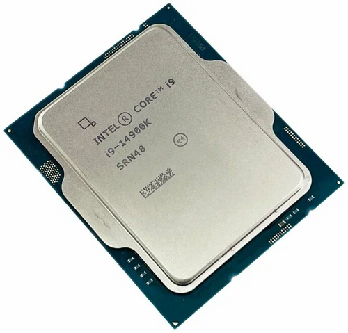
Intel Core は、 Intel Corporationが販売する、ミッドレンジ、組み込み、ワークステーション、ハイエンド、および愛好家向けコンピュータ市場向けのマルチコア(Core Solo および Core 2 Solo を除く)中央処理装置(CPU)のラインです。これらのプロセッサは、導入時に既存のミッドレンジからハイエンドのPentiumプロセッサに取って代わり、Pentium をエントリー レベルに押し上げました。Core プロセッサの同一またはより高性能なバージョンは、サーバーおよびワークステーション市場向けのXeonプロセッサとしても販売されています。
Core は、シングルコア モデルとデュアルコア モデルで構成されるモバイル専用シリーズとして 2006 年 1 月に発売されました。その後、7 月後半に Core 2 シリーズが発売され、最大 4 つのコアを持つデスクトップ プロセッサとモバイル プロセッサの両方が含まれ、64 ビット サポートが導入されました。
2008 年以降、Intel は Core 2 の後継として、Core i3、Core i5、Core i7、Core i9 のプロセッサ ラインナップを導入し始めました。
2023 年に新しい命名スキームが導入され、メインストリーム プロセッサには Core 3、Core 5、Core 7 が使用され、"プレミアム" ハイエンド プロセッサには Core Ultra 5、Core Ultra 7、Core Ultra 9 が使用されます。
概要
Intel Core は内部の一貫性や継続性を約束しないブランドですが、このファミリー内のプロセッサは、大部分がほぼ同様です。
この指定を受けた最初の製品は、65 nmで製造され、2006 年 1 月に市場に投入された、 Pentium M設計ツリーのモバイル向け Core Solo および Core Duo Yonahプロセッサでした。これらは、 Pentium 4より前のPentium Pro系統から派生したもので、Intel Core 製品グループの他の製品とは設計が大きく異なります。
最初の Intel Core デスクトップ プロセッサ (および典型的なファミリ メンバー) は、2006 年 7 月に市場に投入された 65 nm デュアル コア設計のConroeイテレーションから生まれました。これは、マイクロアーキテクチャの効率とパフォーマンスが大幅に強化されたIntel Core マイクロアーキテクチャに基づいており、大幅に低いクロック レートで動作しながら、全般的に (またはそれに近い) Pentium 4 を上回るパフォーマンスを発揮します。深くパイプライン化され、リソースが豊富なアウトオブオーダー実行エンジンでサイクルあたりの命令数(IPC)を高く維持することは、それ以来 Intel Core 製品グループの一貫した特徴となっています。
マイクロアーキテクチャの新たな大幅な進歩は、2008 年 11 月にNehalem アーキテクチャに基づく 45 nm Bloomfieldデスクトップ プロセッサが導入されたことで実現しました。このプロセッサの主な利点は、新しいIntel QuickPath Interconnectと、最大 3 チャネルのDDR3メモリをサポートする統合メモリ コントローラを備えた再設計された I/O およびメモリ システムにあります。
その後のパフォーマンスの向上は、2011 年 1 月に 32 nm で初めてリリースされたSandy BridgeにAdvanced Vector Extensions (AVX) 命令セット拡張機能を追加するなど、大幅な変更よりも追加を行う傾向がありました。また、時間の経過とともに、仮想化のサポートが改善され、 Intel Active Management Technology (iAMT)などの機能の継続的な進化を通じて、システム統合と管理機能のレベルが向上する傾向 (それに伴いパフォーマンスも向上) が生まれました。
2017 年現在、Core ブランドは、エントリー レベルの i3、メインストリームの i5、ハイエンドの i7、および「愛好家」向けの i9 の 4 つの製品ラインで構成されています。Core i7 は 2008 年に導入され、続いて 2009 年に i5、2010 年に i3 が導入されました。最初の Core i9 モデルは 2017 年にリリースされました。
2023年、インテルはプロセッサのブランド名から「i」の名称を削除し、「Core 3/5/7/9」にすると発表しました。同社はハイエンドプロセッサにも「Ultra」ブランドを導入する予定です。[1]新しい命名スキームは、2024年にRaptor Lake-U RefreshとMeteor Lakeプロセッサの発売とともにデビューし、メインストリームプロセッサには「Core 3/5/7」ブランドが使用され、「プレミアム」ハイエンドプロセッサには「Core Ultra 5/7/9」ブランドが使用されました。[2] [3]
- ^ Cypress Coveをベースにした Rocket Lake はCPU マイクロアーキテクチャであり、10 nm 用に設計され、14 nm にバックポートされた Sunny Cove マイクロアーキテクチャのバリエーションです。
- ^ クライアントで 1.25 MB
- ^ 56はアイビーブリッジに統合されました
Intel Core サブブランドのロゴ、2020 年 (第 11 世代のリリースと同時期) から 2023 年まで
-
 Intel Core i3 ロゴ
 -
 Intel Core i5 ロゴ
 -
 Intel Core i7 ロゴ
 -
 Intel Core i9 ロゴ
.svg/500px-Intel_Core_i3_(11th_generation,_logo).svg.png)
.svg/500px-Intel_Core_i5_(11th_generation,_logo).svg.png)
.svg/500px-Intel_Core_i7_(11th_generation,_logo).svg.png)
.svg/500px-Intel_Core_i9_(11th_generation,_logo).svg.png)
2023年から現在までのIntel Coreサブブランドロゴ(2024年初頭のRaptor Lake-U Refreshで正式にリリース)
-
 Intel Core 3 ロゴ
 -
 Intel Core 5 ロゴ
 -
 Intel Core 7 ロゴ
Intel Core Ultra サブブランド ロゴ、2023 年から現在まで ( 2023 年後半にMeteor Lakeで正式にリリース)
-
 Intel Core Ultra 5 ロゴ
 -
 Intel Core Ultra 7 ロゴ
 -
 Intel Core Ultra 9 ロゴ
製品ラインナップ
コア
オリジナルのCoreブランドは、 Pentium Mブランドのプロセッサから派生したIntel の32 ビットモバイルデュアルコア x86 CPU を指します。プロセッサ ファミリは、P6 マイクロアーキテクチャの拡張バージョンを使用しています。これは、 Pentium 4ブランドのNetBurst マイクロアーキテクチャ(Intel P68)と並行して登場し、Core 2 ブランドの CPU の 64 ビットCore マイクロアーキテクチャの前身となりました。Core ブランドには、 Duo (デュアルコア) とSolo (シングルコア、シングルコア モバイル プロセッサの Pentium M ブランドに代わる) の 2 つのブランチがありました。
Intel は、2006 年 1 月 6 日に 32 ビットYonah CPUのリリースとともに Core ブランドを立ち上げました。これは、 Intel 初のデュアルコア モバイル (低電力) プロセッサです。そのデュアルコア レイアウトは、2 つの相互接続されたPentium Mブランドの CPU が 1 つのダイ(ピース) シリコン チップ ( IC ) としてパッケージ化されたものによく似ています。そのため、Core ブランドの CPU の 32 ビット マイクロアーキテクチャは、その名前に反して、その後のCore 2ブランドの CPU の64 ビットCore マイクロアーキテクチャよりも、Pentium M ブランドの CPU との共通点が多くありました。2006 年 1 月からIntelが大規模なブランド変更に取り組んだにもかかわらず、一部の企業は Yonah コアを Pentium M としてマークしたコンピュータの販売を続けました。
Core シリーズは、 Apple Macintoshコンピュータに使用された最初の Intel プロセッサでもあります。Core Duo は第 1 世代MacBook Proの CPU であり、Core Solo は Apple のMac Miniシリーズに登場しました。Core Duo は、Apple がMac シリーズ全体で Intel プロセッサへの移行を開始したことを象徴しています。
2007 年、Intel は主流のモバイル コンピューター向けの Yonah CPU をPentium Dual-Coreとしてブランド化し始めました。これは、同じく Pentium Dual-Core としてブランド化されているデスクトップ 64 ビット Core マイクロアーキテクチャ CPU と混同しないようにするためです。
2007年9月と2008年1月4日には、Core Solo、Core Duo、Celeron、Core 2 Quad製品を含むCoreブランドのCPUの多くが生産中止となった。 [19] [20]
コアソロ
Intel Core Solo [21] (製品コード 80538) は、Core Duo と同じ 2 コア ダイを使用していますが、アクティブなコアは 1 つだけです。需要に応じて、Intel はコアの 1 つを無効にして、Core Solo の価格でチップを販売することもあります。これは、物理的に 1 つのコアしかない別の CPU ラインを立ち上げて維持するよりも労力が少なくて済みます。Intel は以前、486 CPU でも同じ戦略を採用しており、初期の486SX CPU は実際にはFPU を無効にした486DX CPUとして製造されていました。
コアデュオ
Intel Core Duo [22](製品コード80539)は、1つのダイに2つのコア、 両方のコアで共有される2MBのL2キャッシュ、およびL2キャッシュとFSB(フロントサイドバス)アクセスの両方を制御するアービタバスで構成されています。
コア2
Coreの後継は、Coreマイクロアーキテクチャに基づくCore 2ラインのプロセッサのモバイルバージョンであり、 [23] 2006年7月27日にリリースされました。モバイルバージョンのIntel Core 2のリリースは、Intelのデスクトップおよびモバイル製品ラインの再統合を示しています。Core 2プロセッサは、ノートブックのみを対象としていた最初のIntel Core CPUとは異なり、デスクトップとノートブック向けにリリースされました(ただし、 iMacやMac Miniなどの一部の小型フォームファクタおよびオールインワンデスクトップでは使用されました)。
オリジナルの Core とは異なり、Intel Core 2 は 64 ビット プロセッサで、Intel Extended Memory 64 Technology (EM64T) をサポートしています。オリジナルの Core Duo と新しい Core 2 Duo のもう 1 つの違いは、レベル 2 キャッシュの量が増加したことです。新しい Core 2 Duo では、オンボード キャッシュの量が 3 倍の 6 MB になりました。Core 2 では、シングル コアおよびデュアル コア チップにクアッド コア パフォーマンス バリアント (Core 2 Quad ブランド) と、マニア向けバリアントである Core 2 Extreme も導入されました。3 つのチップはすべて 65 nm リソグラフィーで製造され、 2008 年には 45 nm リソグラフィーが導入され、533 MT/s から 1.6 GT/s のフロント サイド バス速度をサポートしています。さらに、Core マイクロアーキテクチャの 45 nm ダイ シュリンクにより、45 nm リソグラフィーで製造されたすべての Core 2 マイクロプロセッサにSSE4.1サポートが追加され、プロセッサの計算速度が向上しました。
コア2ソロ
2007年9月に発表されたCore 2 Solo [24]はCore Soloの後継機で、5.5ワットの熱設計電力を備えた超低消費電力モバイルプロセッサとしてのみ提供されています。オリジナルのU2xxxシリーズ「Merom-L」は、CPUID番号10661(モデル22、ステッピングA1)のMeromチップの特別バージョンを使用していました。これはシングルコアのみを備えており、一部のCeleronプロセッサにも使用されていました。後のSU3xxxは、IntelのCULVプロセッサシリーズの一部で、より小さなμFC-BGA 956パッケージに収められていますが、デュアルコアバリアントと同じPenrynチップが含まれており、製造中にコアの1つが無効になっています。
コア2デュオ

デスクトップおよびモバイルのCore 2プロセッサのバリエーションの大部分は、単一のMerom、Conroe、Allendale、Penryn、またはWolfdaleチップに2つのプロセッサコアを搭載したCore 2 Duo [25] [26]です。これらには、比較的低速の超低電力Uxxxx(10W)および低電力Lxxxx(17W)バージョンから、よりパフォーマンス重視のPxxxx(25W)およびTxxxx(35W)モバイルバージョン、Exxxx(65W)デスクトップモデルまで、幅広いパフォーマンスと消費電力があります。名前に「S」のプレフィックスが付いたモバイルCore 2 Duoプロセッサは、よりコンパクトなラップトップを構築できる、より小さなμFC-BGA 956パッケージで製造されています。
各ラインでは、数字が大きいほどパフォーマンスが良いことを表しますが、これは主にコアとフロントサイドバスのクロック周波数、およびモデル固有の第 2 レベル キャッシュの量によって決まります。Core 2 Duo プロセッサは通常、チップの特定のステッピングで使用可能な 2、3、4、または 6 MB の完全な L2 キャッシュを使用しますが、製造中にキャッシュの量を減らしたバージョンは、 CeleronまたはPentium デュアルコアプロセッサとしてローエンドの消費者市場向けに販売されています。これらのプロセッサと同様に、一部のローエンド Core 2 Duo モデルでは、Intel Virtualization Technologyなどの機能が無効になっています。
コア 2 クアッド
Core 2 Quad [27] [28]プロセッサは、 Core 2 Duoで使用されているものと同様の2つのダイで構成されたマルチチップモジュールで、クアッドコアプロセッサを形成します。これにより、マルチスレッドを活用するシナリオでは、同じクロック周波数でデュアルコアプロセッサの2倍のパフォーマンスが可能になります。
当初、すべての Core 2 Quad モデルは Core 2 Duo デスクトップ プロセッサのバージョンであり、Kentsfield はConroe から、Yorkfield はWolfdale から派生していましたが、後にモバイル デュアル コア Penryn のハイエンド バージョンとして Penryn-QCが追加されました。
Xeon 32xx および 33xx プロセッサは、デスクトップ Core 2 Quad プロセッサとほぼ同じバージョンであり、互換性があります。
コア2エクストリーム
Core 2 Extremeプロセッサ[29] [30]は、Core 2 DuoプロセッサとCore 2 Quadプロセッサの愛好家向けバージョンであり、通常はクロック周波数が高く、クロック乗数がロック解除されているため、オーバークロックに特に適しています。これは、 Extreme Editionとラベル付けされた以前のPentium Dプロセッサに似ています。Core 2 Extremeプロセッサは通常バージョンよりもはるかに高い価格でリリースされ、多くの場合999ドル以上でした。
コアi3/i5/i7/i9
第1世代
2008年11月のNehalemマイクロアーキテクチャのリリースに伴い、[31] IntelはCoreプロセッサの新しい命名方式を導入しました。Core i3、Core i5、Core i7の3つのバリエーションがありますが、名前はコア数などの特定の技術的特徴に対応しなくなりました。代わりに、ブランドは現在、低レベル(i3)、ミッドレンジ(i5)、ハイエンドパフォーマンス(i7)に分割されており、[32]これらは、エントリレベルのCeleron(1つ星)およびPentium(2つ星)プロセッサに続く、IntelのIntel Processor Rating [33]の3つ星、4つ星、5つ星に対応しています。 [34]すべてのNehalemベースのプロセッサに共通する機能には、統合DDR3メモリコントローラ、およびプロセッサ上のQuickPathインターコネクトまたはPCI Expressとダイレクトメディアインターフェイスがあり、これらのプロセッサはすべて、コアあたり 256 KB の L2 キャッシュと、最大 12 MB の共有 L3 キャッシュを備えています。新しい I/O 相互接続のため、以前の世代のチップセットとマザーボードは、Nehalem ベースのプロセッサでは使用できなくなりました。
Intelは、 Core 2ブランドの廃止に伴い、Core i3をIntelのパフォーマンスプロセッサラインの新たなローエンドとして計画していました。[35] [36]
最初のCore i3プロセッサは2010年1月7日に発売されました。[37]
最初のNehalemベースのCore i3はClarkdaleベースで、統合GPUと2つのコアを備えていました。[38]同じプロセッサは、構成が若干異なりますが、Core i5とPentiumとしても利用できます。
Core i3-3xxMプロセッサは、ClarkdaleデスクトッププロセッサのモバイルバージョンであるArrandaleをベースにしている。Core i5-4xxシリーズに似ているが、クロック速度が低く、 Turbo Boostなしで動作する。[39] IntelのFAQによると、エラー訂正コード(ECC)メモリはサポートされていない。[40]マザーボードメーカーのSupermicroによると、Core i3プロセッサをIntel 3400/3420/3450などのサーバーチップセットプラットフォームで使用すると、CPUはUDIMMでECCをサポートする。[41]問い合わせに対し、Intelは、Intel 5シリーズチップセットはCore i5またはi3プロセッサでのみ非ECCメモリをサポートするが、3400シリーズチップセットを搭載したマザーボードでこれらのプロセッサを使用すると、ECCメモリのECC機能をサポートすることを確認した。[42]他社のマザーボードでも、Intel Core ixプロセッサでECCをサポートするものが限られている。 Asus P8B WSはその一例ですが、Windowsの非サーバーオペレーティングシステムではECCメモリをサポートしていません。[43]
Lynnfieldは、 Nehalemマイクロアーキテクチャを採用した最初のCore i5プロセッサであり、2009年9月8日に発表され、以前のCore i7の主流のバリエーションでした。 [44] [45] Lynnfield Core i5プロセッサは、8 MBのL3キャッシュ、2.5 GT/sで動作するDMIバス 、デュアルチャネルDDR3-800/1066/1333メモリのサポートを備えており、ハイパースレッディングは無効になっています。異なる機能セット(ハイパースレッディングと他のクロック周波数)が有効になっている同じプロセッサは、 Core i7-8xxおよびXeon 3400シリーズプロセッサとして販売されていますが、 Bloomfieldに基づくハイエンドのCore i7-9xxおよびXeon 3500シリーズプロセッサと混同しないようにする必要があります。Turbo Boost Technologyと呼ばれる新機能が導入され、要求の厳しいアプリケーションの速度が最大化され、ワークロードに合わせてパフォーマンスが動的に加速されます。
Nehalemが32nmのWestmereダイシュリンクを受けた後、デュアルコアのモバイルCore i5プロセッサであるArrandaleとそのデスクトップ版であるClarkdaleが、同じアーキテクチャに基づくCore i7-6xxおよびCore i3-3xxプロセッサとともに2010年1月に導入された。Arrandaleプロセッサには統合グラフィックス機能がある。Core i3-3xxはTurbo Boostをサポートせず、Core i5-5xxプロセッサのL3キャッシュは3MBに削減されるが、Core i5-6xxはフルキャッシュを使用する。[46] Clarkdaleは、関連するCore i3およびPentiumプロセッサとともにCore i5-6xxとして販売されている。ハイパースレッディングが有効で、完全な4MBのL3キャッシュを備えている。[47]
Intelによると、「Core i5デスクトッププロセッサとデスクトップボードは通常ECCメモリをサポートしていません」[48]が、Core i3セクションの限定的なECCサポートに関する情報はCore i5とi7にも適用されます。[引用が必要]
Core i7ブランドは、デスクトップおよびラップトップコンピュータの両方のビジネスおよびハイエンド消費者市場をターゲットにしており、[50] Core i3(エントリーレベルの消費者)、Core i5(主流の消費者)、およびXeon (サーバーおよびワークステーション)ブランドとは区別されています。
2008年後半に発表されたブルームフィールドは、 Nehalemアーキテクチャをベースにした最初のCore i7プロセッサでした。[51] [52] [53] [54]翌年、リンフィールドのデスクトッププロセッサとクラークスフィールドのモバイルプロセッサは、このアーキテクチャをベースにした新しいクアッドコアCore i7モデルを発表しました。[55]
Nehalemが 32 nm Westmereダイ シュリンクを採用した後、 2010 年 1 月にArrandaleデュアルコア モバイル プロセッサが導入され、続いて 2010 年 3 月 16 日に Core i7 初の 6 コア デスクトップ プロセッサGulftownが導入されました。通常の Core i7 とExtreme Edition はどちらも、Intel プロセッサ レーティングで 5 つ星として宣伝されています。
第 1 世代の Core i7では、ハイエンドのデスクトップおよびサーバー向けに設計されたLGA 1366と、ローエンドおよびミッドエンドのデスクトップおよびサーバーで使用されるLGA 1156の 2 つの異なるソケットが使用されています。各世代において、最高性能の Core i7 プロセッサは、その世代のミッドエンド Xeon プロセッサと同じソケットとQPIベースのアーキテクチャを使用し、低性能の Core i7 プロセッサは Core i5 と同じソケットと PCIe/DMI/FDI アーキテクチャを使用しています。
「Core i7」はIntel Core 2ブランドの後継である。[56] [57] [58] [59] Intelの代表者は、将来IntelがNehalemベースの新しい製品をリリースする際に、消費者がどのプロセッサを購入するかを決定するのに役立つように、 Core i7という名称 を意図したと述べた。[60]
第2世代
2011年初頭、IntelはSandy Bridgeという新しいマイクロアーキテクチャを発表しました。これはCoreプロセッサマイクロアーキテクチャの第2世代です。Core i3/i5/i7を含むNehalemの既存のブランドはすべて維持され、新しいモデル番号が導入されました。Sandy Bridgeプロセッサの最初のセットにはデュアルコアとクアッドコアのバリアントが含まれており、それらはすべて、以前のマイクロアーキテクチャとは異なり、CPUと統合GPUコアの両方に単一の32nmダイを使用しています。Sandy Bridgeマイクロアーキテクチャを備えたすべてのCore i3/i5/i7プロセッサには、4桁のモデル番号があります。モバイルバージョンでは、熱設計電力は1文字または2文字のサフィックスから判断できなくなりましたが、CPU番号にエンコードされています。Sandy Bridge以降、Intelはコア数、ソケット、または使用目的に基づいてプロセッサのコード名を区別しなくなりました。
Ivy Bridge は、2012 年 4 月に導入された、トライゲート (「3D」) トランジスタに基づく Intel の Sandy Bridge マイクロアーキテクチャの 22 nm ダイ シュリンクのコード名です。
2011 年 1 月 20 日にリリースされたデスクトップおよびモバイル プロセッサの Core i3-2xxx ラインは、新しいマイクロアーキテクチャに基づく、2010 年の「Clarkdale」Core i3-5xx および「Arrandale」Core i3-3xxM モデルの直接的な代替品です。新しいソケットとチップセットが必要ですが、Turbo BoostおよびAES-NIのサポートがないなど、Core i3 のユーザーに見える機能はほとんど変更されていません。Sandy Bridge ベースの Celeron および Pentium プロセッサとは異なり、Core i3 ラインは新しいAdvanced Vector Extensions をサポートしています。この特定のプロセッサは、この新しい Intel プロセッサ シリーズのエントリー レベル プロセッサです。

2011 年 1 月、Intel は CES 2011 で「Sandy Bridge」マイクロアーキテクチャに基づく新しいクアッドコア Core i5 プロセッサを発表しました。新しいデュアルコア モバイル プロセッサとデスクトップ プロセッサは 2011 年 2 月に登場しました。
Core i5-2xxx シリーズのデスクトップ プロセッサは、デュアル コア Core i5-2390T を除き、ほとんどがクアッド コア チップで、統合グラフィックスを搭載し、以前の Core i5-6xx および Core i5-7xx シリーズの主要機能を組み合わせています。4 桁のモデル番号の後の接尾辞は、ロック解除された乗数 (K)、低電力 (S)、および超低電力 (T) を表します。
現在、デスクトップ CPU はすべて、i5-2390T を除いて、4 つの非SMTコア (i5-750 など) を備えています。DMI バスは 5 GT/s で動作します。
モバイル Core i5-2xxxM プロセッサは、以前の Core i5-5xxM シリーズと同様にデュアルコアおよびハイパースレッド チップであり、その製品ラインとほとんどの機能を共有しています。
Core i7 ブランドは、2017 年に i9 が発表されるまで、Intel のデスクトップおよびモバイル プロセッサのハイエンドでした。その Sandy Bridge モデルは、最大の L3 キャッシュと最高のクロック周波数を特徴としています。これらのモデルのほとんどは、より小型の Core i5 の兄弟モデルと非常によく似ています。クアッドコア モバイル Core i7-2xxxQM/XM プロセッサは、以前の「Clarksfield」Core i7-xxxQM/XM プロセッサを継承していますが、統合グラフィックスも搭載されています。
第3世代
Ivy Bridge は、Intel が開発した 22 nm 製造プロセスに基づく「第 3 世代」プロセッサ ラインのコード名です。CPU のモバイル バージョンは 2012 年 4 月にリリースされ、デスクトップ バージョンは 2012 年 9 月にリリースされました。
Ivy Bridge ベースの Core-i3-3xxx ラインは、22 nm プロセス テクノロジーとより優れたグラフィックスへのマイナー アップグレードです。
第4世代
Haswell は第 4 世代 Core プロセッサ マイクロアーキテクチャであり、2013 年にリリースされました。
第5世代
Broadwellは第5世代Coreプロセッサマイクロアーキテクチャであり、Intelによって2014年9月6日にリリースされ、2014年後半に出荷が開始されました。14nmチップを使用する最初のチップです。[62]さらに、モバイルプロセッサは2015年1月に発売され[63]、デスクトップCore i5およびi7プロセッサは2015年6月にリリースされました。[64]
デスクトップ プロセッサ (DT シリーズ)
モバイル プロセッサ (U シリーズ)
モバイル プロセッサ (Y シリーズ)
第6世代
Broadwell マイクロアーキテクチャ
Skylakeマイクロアーキテクチャ
Skylake は第 6 世代 Core プロセッサ マイクロアーキテクチャであり、2015 年 8 月に発売されました。Broadwell ラインの後継として、同じ 14 nm 製造プロセス技術を使用して再設計されていますが、再設計により CPU と GPU のパフォーマンスが向上し、消費電力が削減されています。Intel は、非 K プロセッサのオーバークロックも無効にしました。
第7世代
Skylakeマイクロアーキテクチャ
ケイビー湖
Kaby Lakeは第7世代Coreプロセッサのコードネームで、2016年10月(モバイルチップ)[65]と2017年1月(デスクトップチップ)[66]に発売されました。最新世代のマイクロアーキテクチャでは、Intelは「ティック・トック」製造設計モデルを使用せずにKaby Lakeプロセッサを製造することを決定しました。[67] Kaby LakeはSkylakeと同じマイクロアーキテクチャを採用しており、Intelの14ナノメートル製造プロセス技術を使用して製造されています。 [67]
改良された 14 nm プロセス (14FF+) に基づいて構築された Kaby Lake は、より高速な CPU クロック速度とTurbo周波数を特徴としています。これらのプロセスとクロック速度の変更以外では、CPU アーキテクチャはSkylakeからほとんど変更されておらず、IPC は同一です。
Kaby Lake は、 3D グラフィックスと4K ビデオ再生のパフォーマンスを向上させる新しいグラフィックス アーキテクチャを備えています。ネイティブのHigh-bandwidth Digital Content Protection 2.2 サポートが追加され、 H.264/MPEG-4 AVC、High Efficiency Video Coding Main および Main10/10 ビット、VP9 10 ビットおよび 8 ビット ビデオの固定機能デコードもサポートされます。ハードウェア エンコードは、H.264/MPEG-4 AVC、 HEVC Main10/10 ビット、VP9 8 ビット ビデオでサポートされます。VP9 10 ビット エンコードはハードウェアではサポートされません。OpenCL 2.1がサポートされるようになりました。
Kaby Lake は、Pentium ブランドのデスクトップ CPU SKU で ハイパースレッディングをサポートする最初の Core アーキテクチャです。Kaby Lake には、オーバークロックに対応した最初の i3 ブランド CPU も搭載されています。
デスクトップ Kaby Lake CPU に共通する機能:
- LGA 1151ソケット
- DMI 3.0およびPCIe 3.0インターフェース
- 次の構成でのデュアル チャネル メモリ サポート: DDR3L-1600 1.35 V (最大 32 GiB) または DDR4-2400 1.2 V (最大 64 GiB)
- 合計16個のPCIeレーン
- CoreブランドのプロセッサはAVX2命令セットをサポートしています。CeleronおよびPentiumブランドのプロセッサはSSE4.1/4.2のみをサポートしています。
- 350 MHz ベースグラフィッククロックレート
- L4 キャッシュ (eDRAM) なし。
- 発売日は2017年1月3日
Kaby Lake-X プロセッサは、LGA 2066 ソケットに適合する Kaby Lake-S プロセッサの改良版です。ただし、プラットフォームの独自の機能は利用できません。
第8世代
ケイビー湖リフレッシュ
Coffee Lake マイクロアーキテクチャ
Coffee Lake は、第 8 世代 Intel Core ファミリーのコード名であり、2017 年 10 月に発売されました。Intel Core プロセッサーの 10 年の歴史の中で初めて、Coffee Lake 世代ではデスクトップ プロセッサー ラインアップ全体でコア数が増加し、クロックあたりのパフォーマンスは同様であるにもかかわらず、前世代と比較してパフォーマンスが大幅に向上しました。
* Intelハイパースレッディング機能により、対応プロセッサは物理コアごとに2つのスレッドを実行できます。
Coffee Lakeは、Skylake/Kaby Lakeとほぼ同じCPUコアとMHzあたりの性能を備えています。[68] [69] Coffee Lake特有の機能には以下のものがあります。
- Skylake および Kaby Lake の 14 nm プロセスと同様の改良に続き、Coffee Lake は 3 番目の 14 nm プロセス改良 (「14nm++」) であり、トランジスタ ゲート ピッチの拡大により電流密度が低下し、トランジスタのリークが増加し、ダイ領域とアイドル電力を犠牲にしてピーク電力と周波数が高くなります。
- Coffee Lakeは300シリーズチップセットと組み合わせて使用され、古い100シリーズおよび200シリーズチップセットとは互換性がありません。[70] [71]
- コア数に応じてL3キャッシュを増加
- i5 および i7 CPU モデル全体でターボ クロック速度が向上 (最大 200 MHz 増加)
- iGPUクロック速度を50MHz向上
- DDR4メモリのサポートが2666 MHz(i5およびi7パーツの場合)および2400 MHz(i3パーツの場合)に更新されました。DDR3メモリはサポートされなくなりました。
* プロセッサCore i3-8100およびCore i3-8350K(B0ステッピング)は、実際には「Kaby Lake-S」ファミリー に属します。
Amber Lake マイクロアーキテクチャ
Amber Lake は、低電力の Mobile Kaby Lake CPU を改良したものです。
ウィスキーレイクマイクロアーキテクチャ
Whiskey Lakeは、Kaby Lake RefreshとCoffee Lakeに続く、 Intelの3番目の14nm Skylakeプロセス改良のコードネームです。Intelは、2018年8月28日に低電力モバイルWhiskey Lake CPUの提供開始を発表しました。 [73] [74]このCPUアーキテクチャにMeltdown / Spectreクラスの脆弱性に対するハードウェア緩和策が含まれているかどうかはまだ宣伝されていません。さまざまな情報源に矛盾する情報が含まれています。[75] [76] [74] [77]非公式には、Whiskey LakeにはMeltdownとL1TFに対するハードウェア緩和策があり、Spectre V2にはソフトウェア緩和策とマイクロコード/ファームウェアの更新が必要であると発表されました。[78] [79] [80] [81]
キャノンレイクマイクロアーキテクチャ
Cannon Lake(旧称Skymont)は、 Kaby Lakeマイクロアーキテクチャの10ナノメートルダイシュリンクに対するIntelのコードネームである。ダイシュリンクとしてのCannon Lakeは、半導体製造の次のステップとしてのIntelの「プロセス-アーキテクチャ-最適化」実行計画における新しいプロセスである。 [82] Cannon Lakeは、 AVX-512命令セットを含む最初の主流CPUである。前世代のAVX2(AVX-256)と比較して、新世代のAVX-512は、データレジスタの幅とレジスタの数が最も2倍になっている。これらの機能強化により、レジスタの幅が広がったことでレジスタあたりの浮動小数点演算の数が2倍になり、レジスタの総数も2倍になり、理論上のパフォーマンスはAVX2の最大4倍に向上する。[83] [84]
CES 2018で、インテルは2017年末にモバイルCannon Lake CPUの出荷を開始し、2018年には生産を増強すると発表した。 [85] [86] [87]それ以上の詳細は明らかにされていない。
第9世代
Skylakeマイクロアーキテクチャ
第 9 世代 Coffee Lake CPU は、クロック速度が向上した以前の Skylake X シリーズ CPU の更新バージョンです。
Coffee Lake Refresh マイクロアーキテクチャ
第9世代Coffee Lake CPUは2018年第4四半期にリリースされました。これらには、特定のMeltdown / Spectre脆弱性に対するハードウェア緩和策が含まれています。[90] [91]
これらのCPUは、Intelのコンシューマー向けCPU史上初めて、最大128GBのRAMをサポートします。[92]
* Intelハイパースレッディング機能により、対応プロセッサは物理コアごとに2つのスレッドを実行できます。
FサフィックスのCPUには統合GPUが搭載されていないにもかかわらず、IntelはこれらのCPUの価格を機能豊富なCPUと同じ価格に設定しました。[93]
* さまざまなレビューによると、Core i9 9900K CPUは負荷がかかると140W以上を消費する可能性がある。Core i9 9900KSはさらに多く消費する可能性がある。[95] [96] [97] [98]
第10世代
Cascade Lake マイクロアーキテクチャ
Cascade Lake X シリーズ CPU は、以前の Skylake X シリーズ CPU の第 10 世代バージョンです。クロック速度がわずかに向上し、価格が大幅に引き下げられています。
Ice Lake マイクロアーキテクチャ
Ice Lake は、Intel の第 10 世代 Intel Core プロセッサのコード名であり、前世代の Kaby Lake/Cannon Lake プロセッサの「アーキテクチャ」の強化を表しています (Intel のプロセス アーキテクチャ最適化実行計画で指定されているとおり)。Cannon Lake の後継として、Ice Lake は Intel の新しい 10 nm+ 製造プロセスを使用し、Sunny Cove マイクロアーキテクチャを搭載しています。
Ice Lake は、2017 年に発見されたハードウェア脆弱性であるMeltdownとSpectre に対するシリコン内緩和策を備えた最初の Intel CPU です。これらのサイドチャネル攻撃は、分岐予測の投機的実行の使用を悪用します。これらのエクスプロイトにより、CPU は、タイミング攻撃の形で、エクスプロイト プロセスがアクセスできないように意図されたキャッシュされたプライベート情報を明らかにする可能性があります。[引用が必要]
Comet Lake マイクロアーキテクチャ
Comet Lakeは、 Whiskey Lakeに続く、 Intelの4番目の14nm Skylakeプロセス改良版のコードネームです。Intelは、2019年8月21日に低電力モバイルComet Lake CPUの提供を発表しました。[99]
Comet Lake Refresh マイクロアーキテクチャ
Amber Lake Refresh マイクロアーキテクチャ
第11世代
タイガーレイク
2020年9月2日に発売されました。
- 全モデルDDR4-3200メモリをサポート
- すべてのモデルは20個の再構成可能なPCI Express 4.0レーンをサポートし、ディスクリートGPU用のx16 Gen 4リンクとM.2 SSD用のx4 Gen 4リンクを可能にします。
モバイルプロセッサ(Tiger Lake-H)
モバイルプロセッサ(Tiger Lake-H35)
- すべてのモデルはDDR4-3200またはLPDDR4X-4267メモリをサポートしています
モバイルプロセッサ(UP3クラス)
モバイルプロセッサ(UP4クラス)
デスクトップ/タブレット プロセッサ (Tiger Lake-B)
- ソケット: FCBGA1787、BGAソケット。したがって、これらのCPUはシステムインテグレーター専用です。
- インテル Xe UHD グラフィックス
- 最大128 GB DDR4-3200メモリ
- 当初はTVBブースト周波数が5.3GHzであると誤って記載されていました。[101]
Rocket Lake マイクロアーキテクチャ
Rocket Lakeは、新しいCypress Coveマイクロアーキテクチャに基づくIntelのデスクトップx86チップファミリーのコードネームであり、Sunny Cove(IntelのIce Lakeモバイルプロセッサで使用)のバリアントを古い14nmプロセスにバックポートしたものです。[102]このチップは「Intel第11世代Core」として販売されています。2021年3月30日に発売されました。
デスクトッププロセッサ
- 以下にリストされているすべてのCPUは、DDR4-3200をネイティブでサポートしています。Core i9 K/KFプロセッサは、DDR4-3200でデフォルトでDRAMとメモリコントローラの比率を1:1にしますが、Core i9 non K/KFおよび以下にリストされている他のすべてのCPUは、DDR4-3200でデフォルトでDRAMとメモリコントローラの比率を2:1にし、DDR4-2933でデフォルトで1:1にします。[103]
- すべてのCPUはデュアルチャネルモードで最大128GiBのRAMをサポートします。
- Core i9 CPU(11900Tを除く)はIntel Thermal Velocity Boostテクノロジーをサポート
第12世代
アルダー湖
Alder Lakeは、Golden Cove高性能コアとGracemont省電力コアを活用したハイブリッドアーキテクチャに基づく第12世代Intel CoreプロセッサのIntelコード名です。[104]
これは、以前はIntel 10 nm Enhanced SuperFin(10ESF)と呼ばれていた
IntelのIntel 7
プロセスを使用して製造されています。Intel
は2021年10月27日に第12世代Intel Core CPUを正式に発表し、2021年11月4日に市場に投入されました。[105]
デスクトップ プロセッサ (Alder Lake-S)
- 全てのCPUはデュアルチャネルモードで最大128GBのDDR4-3200またはDDR5-4800 RAMをサポートします。[106]
- 一部のモデルには、32/24/16 EU と 300 MHz の基本周波数を備えた統合型UHD Graphics 770、UHD Graphics 730、またはUHD Graphics 710 GPU が搭載されています。
- デフォルトでは、Alder Lake CPUは常にTurbo Powerで動作するように設定されており、Pコア/Eコアがベースクロックレートを超えない場合にのみBase Powerが保証されます。 [107]
- 最大ターボ電力: 電流および/または温度制御によって制限されるプロセッサの最大持続電力 (> 1 秒)。瞬間電力は、短時間 (≤ 10 ミリ秒) に最大ターボ電力を超える場合があります。最大ターボ電力は、システム ベンダーによって構成可能であり、システム固有の値になる場合があります。
- 下記の太字のCPUは、W680チップセットをベースにしたマザーボードと組み合わせた場合にのみECCメモリをサポートします。 [108]
*デフォルトでは、Core i9 12900KSはThermal Velocity Boostを使用している場合にのみ5.5GHzを達成します[109]
超高性能モバイル プロセッサ (Alder Lake-HX)
- 太字はECCメモリのサポートを示します
高性能モバイルプロセッサ (Alder Lake-H)
低消費電力パフォーマンス モバイル プロセッサ (Alder Lake-P)
超低消費電力モバイル プロセッサ (Alder Lake-U)
第13世代
ラプター湖
Raptor Lakeは、Intelの第13世代Coreプロセッサとハイブリッドアーキテクチャに基づく第2世代のコードネームです。[111] Intelの
Intel 7プロセス
の改良版を使用して製造されています。 [112] Intelは2022年10月22日にRaptor Lakeを発売しました。
デスクトップ プロセッサ (Raptor Lake-S)
- すべてのCPUは最大DDR5 4800および192 GiBのRAMをサポートします
- 13600以上DDR5 5600をサポート
- 13500以下はDDR5 4800をサポート
- LGA 1700 による Intel 600 および 700 チップセットのサポート
- Intel 600シリーズチップセットでは、Raptor Lake-Sのサポートを実現するためにBIOSアップデートが必要です。
- 最初の 6 GHz プロセッサ (13900KS)*
*デフォルトでは、Core i9 13900KS は、十分な電力と冷却を備えた Thermal Velocity Boost を使用している場合にのみ 6.0 GHz を達成します。
第14世代
ラプターレイクリフレッシュ
Raptor Lake Refreshは、第14世代Intel CoreプロセッサーのIntelコード名です。これはリフレッシュであり、第13世代と同じアーキテクチャに基づいており、Core i9 14900KSで最大6.2GHz、Core i9 14900Kと14900KFで6GHz、Core i7 14700Kと14700KFで5.6GHz、Core i5 14600Kと13400KFで5.3GHzのクロック速度と、非FプロセッサーのUHDグラフィックス770を備えています。これらはまだIntel 7プロセスノードに基づいています。[113] 2023年10月17日に発表されたこれらのCPUは、600および700シリーズのマザーボードとの互換性を可能にするLGA 1700ソケット用に設計されています。[114] Intelは2023年に将来のIntel Coreプロセッサから「i」プレフィックスを削除すると発表したため、これはIntel Core i3、i5、i7、i9の命名スキームを使用する最後の世代のCPUです。[1]
第14世代CPUはRaptor Lakeに比べてアーキテクチャ上の大きな変更はありませんが、いくつかの小さな改善が加えられています。[115]第14世代CPUは、3D V-Cacheを搭載したAMDのZen 4を打ち負かすための最後の努力として広く批判されました[独自の研究? ] [116] [117] Intelの次世代アーキテクチャのデスクトップバージョンであるMeteor Lakeはキャンセルされ、Arrow Lakeアーキテクチャはまだリリースの準備ができていませんでした。[118]
Raptor Lake-S Refreshデスクトッププロセッサに加えて、Intelは2024年1月に第14世代Raptor Lake-HX Refreshモバイルプロセッサも発売しました。[119]
以下の太字の CPU は、それぞれの Intel Ark 製品ページに従って W680 チップセットをベースにしたマザーボードと組み合わせた場合にのみ、 ECC メモリをサポートします。
Core and Core Ultra 3/5/7/9
Starting with the Meteor Lake mobile series launched in December 2023 (with the exception of Raptor Lake-HX Refresh),[120] Intel introduced a new naming system for its new and upcoming processors. The numbers 3, 5, 7 and 9 which denote tiers are still used, but the letter 'i' is dropped, and there is a new "Core Ultra" sub-brand. Like AMD with their Ryzen 7000 mobile series and later processors, Intel now refreshes older architectures to be sold as more affordable mainstream processors while the latest architectures are released as "premium" products, under the Core Ultra brand.[121]
This new naming system also cuts the number of model number digits down from 4-5 to 3-4, e.g. Core 1xx series instead of Core 8xxx or 14xxx series.
Intel no longer refers to iterations of product series under "nth generation" anymore, instead using "Series n". Otherwise the latest series launched in December 2023 would be called 15th generation.[122]
Series 1
The Series 1 of Core processors consists of the Raptor Lake-U Refresh mobile series released January 2024 under the Core brand,[121] and the Meteor Lake-U/H mobile series released December 2023 under the Core Ultra brand.[120]
Meteor Lake
Meteor Lake is Intel's codename for the first generation of Intel Core Ultra mobile processors,[123] and was officially launched on December 14, 2023.[124] It is the first generation of Intel mobile processors to use a chiplet architecture which means that the processor is a multi-chip module.[123] Tim Wilson led the system on a chip development for this generation microprocessor.[125]
Process technology
Due to its Multi-Chip Module (MCM) construction, Meteor Lake can take advantage of different process nodes that are best suited to the use case. Meteor Lake is built using four different fabrication nodes, including both Intel's own nodes and external nodes outsourced to fabrication competitor TSMC. The "Intel 4" process used for the CPU tile is the first process node in which Intel is utilising extreme ultraviolet (EUV) lithography, which is necessary for creating nodes 7nm and smaller. The interposer base tile is fabricated on Intel's 22FFL, or "Intel 16", process.[126][127] The 22FFL Fin Field-Effect Transistor (FinFET) Low-power node, first announced in March 2017, was designed for inexpensive low power operation.[128] The interposer base tile is designed to connect tiles together and allow for die-to-die communication which does not require the most advanced, expensive nodes so an older, inexpensive node can be used instead.
Mobile processors
Meteor Lake-H
155H, 165H, and 185H support P-core Turbo Boost 3.0 running at the same frequency as Turbo Boost 2.0.
- ^ a b Price is Recommended Customer Price (RCP) at launch. RCP is the trade price that processors are sold by Intel to retailers and OEMs. Actual MSRP for consumers is higher
Meteor Lake-U
The integrated GPU is branded as "Intel Graphics" but still use the same GPU microarchitecture as "Intel Arc Graphics" on the H series models.
All models support DDR5 memory except 134U and 164U.
- ^ Price is Recommended Customer Price (RCP) at launch. RCP is the trade price that processors are sold by Intel to retailers and OEMs. Actual MSRP for consumers is higher
Processors for Internet of Things (IoT) devices and embedded systems (Meteor Lake-PS)
High-power
155HL and 165HL support P-core Turbo Boost 3.0 running at the same frequency as Turbo Boost 2.0.
- ^ Price is Recommended Customer Price (RCP) at launch. RCP is the trade price that processors are sold by Intel to retailers and OEMs. Actual MSRP for consumers is higher
Low-power
The integrated GPU is branded as "Intel Graphics" but still use the same GPU microarchitecture as "Intel Arc Graphics" on the high-power models.
- ^ Price is Recommended Customer Price (RCP) at launch. RCP is the trade price that processors are sold by Intel to retailers and OEMs. Actual MSRP for consumers is higher
Series 2
Lunar Lake
Mobile processors
- ^ Only the P-cores can access this L3 cache[132]
Arrow Lake
Arrow Lake is Intel’s codename for the second generation Core Ultra processors. Announced on October 10, 2024, and released on October 24, 2024, Arrow Lake is the first series of desktop Intel processors not to feature a monolithic design, instead adopting the chiplet design used on Meteor Lake.[133][134] Intel primarily markets this product as being on-par with Raptor Lake in performance whilst being much more power efficient.[135] The processors use the LGA 1851 socket with the 800 series chipset.
Reception
Speculative execution CPU vulnerabilities
Transient execution CPU vulnerabilities are vulnerabilities in which instructions, most often optimized using speculative execution, are executed temporarily by a microprocessor, without committing their results due to a misprediction or error, resulting in leaking secret data to an unauthorized party. The archetype is Spectre, and transient execution attacks like Spectre belong to the cache-attack category, one of several categories of side-channel attacks. Since January 2018 many different cache-attack vulnerabilities have been identified.
See also
- Intel Core (microarchitecture)
- List of Intel graphics processing units
- List of Intel processors
- List of Intel Core processors
- List of Intel chipsets
- Ryzen
- Zen (microarchitecture)
References
- ^ a b Cao, Peter (June 15, 2023). "Intel drops 'i' processor branding after 15 years, introduces 'Ultra' for higher-end chips". Engadget. Retrieved June 17, 2023.
- ^ Bonshor, Gavin (June 15, 2023). "Intel To Launch New Core Processor Branding for Meteor Lake: Drop the i, Add Ultra Tier". AnandTech. Archived from the original on April 5, 2024. Retrieved April 5, 2024.
- ^ Robinson, Cliff (June 15, 2023). "Intel Overhauls Core Branding with Meteor Lake". ServeTheHome. Archived from the original on April 5, 2024. Retrieved April 5, 2024.
- ^ a b c Cutress, Ian. "The Ice Lake Benchmark Preview: Inside Intel's 10nm". www.anandtech.com. Retrieved October 23, 2020.
- ^ "Hiérarchie des caches - L'architecture Intel Nehalem - HardWare.fr". www.hardware.fr. Retrieved October 23, 2020.
- ^ Kanter, David. "Intel's Sandy Bridge Microarchitecture". Retrieved October 24, 2020.
- ^ "Willow Cove - Microarchitectures - Intel - WikiChip". en.wikichip.org. Retrieved October 23, 2020.
- ^ Cutress, Ian; Frumusanu, Andrei. "Intel's Tiger Lake 11th Gen Core i7-1185G7 Review and Deep Dive: Baskin' for the Exotic". www.anandtech.com. Retrieved November 8, 2020.
- ^ "Intel Core i7-5775C - CM8065802483301 / BX80658I75775C". www.cpu-world.com. Retrieved November 6, 2020.
- ^ "Noyau (suite) - L'architecture Intel Nehalem - HardWare.fr". www.hardware.fr. Retrieved October 23, 2020.
- ^ "File:broadwell buffer window.png - WikiChip". en.wikichip.org. Retrieved October 23, 2020.
- ^ "File:sunny cove buffer capacities.png - WikiChip". en.wikichip.org. Retrieved October 23, 2020.
- ^ a b c d e "Popping the Hood on Golden Cove". chipsandcheese.com. December 2, 2021. Retrieved April 12, 2023.
- ^ "Sunny Cove - Microarchitectures - Intel - WikiChip". en.wikichip.org. Retrieved November 4, 2020.
- ^ Kanter, David. "Intel's Sandy Bridge Microarchitecture". Retrieved November 9, 2020.
- ^ a b Shimpi, Anand Lal. "Intel's Haswell Architecture Analyzed: Building a New PC and a New Intel". www.anandtech.com. Retrieved November 9, 2020.
- ^ Cutress, Ian. "Examining Intel's Ice Lake Processors: Taking a Bite of the Sunny Cove Microarchitecture". www.anandtech.com. Retrieved November 9, 2020.
- ^ "Intel launches three Core M CPUs, promises more Broadwell "early 2015"". Ars Technica. September 5, 2014. Archived from the original on January 5, 2015.
- ^ "Intel already phasing out first quad-core CPU". TG Daily. Archived from the original on September 13, 2007. Retrieved September 7, 2007.
- ^ "Intel to discontinue older Centrino CPUs in Q1 08". TG Daily. Archived from the original on November 2, 2007. Retrieved October 1, 2007.
- ^ "Support for the Intel Core Solo processor". Intel. Archived from the original on April 19, 2010. Retrieved December 13, 2010.
- ^ "Support for the Intel Core Duo Processor". Intel. Archived from the original on April 17, 2010. Retrieved December 13, 2010.
- ^ "Intel Microarchitecture". Intel. Archived from the original on June 12, 2009. Retrieved December 13, 2010.
- ^ "Intel Core2 Solo Mobile Processor – Overview". Intel. Archived from the original on September 26, 2011. Retrieved December 13, 2010.
{{cite web}}: CS1 maint: unfit URL (link) - ^ "Intel Core2 Duo Processor: Upgrade Today". Intel. Archived from the original on January 7, 2011. Retrieved December 13, 2010.
- ^ "Intel Core2 Duo Mobile Processor". Intel. Archived from the original on April 3, 2009. Retrieved December 13, 2010.
- ^ "Intel Core2 Quad Processor Overview". Intel. Archived from the original on March 6, 2011. Retrieved December 13, 2010.
{{cite web}}: CS1 maint: unfit URL (link) - ^ "Intel Core2 Quad Mobile Processors – Overview". Intel. Archived from the original on May 6, 2015. Retrieved December 13, 2010.
{{cite web}}: CS1 maint: unfit URL (link) - ^ "Support for the Intel Core2 Extreme Processor". Intel. Archived from the original on March 16, 2010. Retrieved December 13, 2010.
- ^ "Intel Core2 Extreme Processor". Intel. Archived from the original on February 21, 2011. Retrieved December 13, 2010.
{{cite web}}: CS1 maint: unfit URL (link) - ^ "Intel Microarchitecture Codenamed Nehalem". Intel. Archived from the original on July 22, 2010. Retrieved December 13, 2010.
- ^ "Public Roadmap Desktop, Mobile & Data Center" (PDF). Intel. Archived from the original (PDF) on February 5, 2009. Retrieved December 13, 2010.
- ^ "Intel Processor Ratings". Intel. Archived from the original on April 15, 2011. Retrieved July 21, 2011.
- ^ "Processor Ratings". Intel. July 9, 2010. Archived from the original on January 1, 2011. Retrieved December 13, 2010.
- ^ "Intel Quietly Announces Core i5 and Core i3 Branding". AnandTech. Archived from the original on March 23, 2010. Retrieved December 13, 2010.
- ^ "Intel confirms Core i3 as 'entry-level' Nehalem chip". Apcmag.com. September 14, 2009. Archived from the original on September 7, 2011. Retrieved December 13, 2010.
- ^ "Core i5 and i3 CPUs With On-Chip GPUs Launched". Hardware.slashdot.org. January 4, 2010. Archived from the original on January 12, 2012. Retrieved December 13, 2010.
- ^ "Intel May Unveil Microprocessors with Integrated Graphics Cores at Consumer Electronics Show". Xbitlabs.com. Archived from the original on October 30, 2010. Retrieved December 13, 2010.
- ^ "Intel to launch four Arrandale CPUs for mainstream notebooks in January 2010". Digitimes.com. November 13, 2009. Archived from the original on December 7, 2010. Retrieved December 13, 2010.
- ^ "Intel Core i3 Desktop Processor — Frequently Asked Questions". Intel. Archived from the original on September 25, 2011.
- ^ "FAQ Entry – Online Support – Support – Super Micro Computer, Inc". www.Supermicro.com. Archived from the original on July 2, 2017. Retrieved January 5, 2018.
- ^ "SPCR • View topic – ECC Support (offshoot of Silent Server Build)". silentpcreview.com. Archived from the original on January 5, 2012. Retrieved September 26, 2011.
- ^ Asus P8B WS specification Archived September 25, 2011, at the Wayback Machine: supports "ECC, Non-ECC, un-buffered Memory", but "Non-ECC, un-buffered memory only support for client OS (Windows 7, Vista and XP)."
- ^ "Support for the Intel Core i5 Processor". Intel. Archived from the original on April 11, 2010. Retrieved December 13, 2010.
- ^ Anand Lal Shimpi, Intel's Core i7 870 & i5 750, Lynnfield: Harder, Better, Faster Stronger, anandtech.com, archived from the original on July 22, 2011
- ^ "Login to Digitimes archive & research". www.digitimes.com. November 13, 2009. Archived from the original on March 20, 2016. Retrieved May 7, 2018.
- ^ "Intel 奔腾双核 E5300(盒) 资讯-CPU 资讯-新奔腾同现身 多款Core i5、i3正式确认-IT168 diy硬件". it168.com. Archived from the original on October 9, 2011.
- ^ "Intel Core i5 Desktop Processor — Integration, Compatibility, and Memory FAQ". Intel. Archived from the original on February 11, 2012.
- ^ "Intel Core i5-430UM Mobile processor – CN80617006042AE". cpu-world.com. Archived from the original on August 12, 2011.
- ^ "Support for the Intel Core i7 Processor". Intel. Archived from the original on November 29, 2010. Retrieved December 13, 2010.
- ^ Modine, Austin (November 18, 2008). "Intel celebrates Core i7 launch with Dell and Gateway". The Register. Archived from the original on December 20, 2008. Retrieved December 6, 2008.
- ^ "IDF Fall 2008: Intel un-retires Craig Barrett, AMD sets up anti-IDF camp". Tigervision Media. August 11, 2008. Archived from the original on May 25, 2024. Retrieved August 11, 2008.
- ^ "Meet the Bloggers". Intel Corporation. Archived from the original on February 2, 2012. Retrieved August 11, 2008.
- ^ "Getting to the Core – Intel's new flagship client brand". Intel Corporation. Archived from the original on August 18, 2008. Retrieved August 11, 2008.
- ^ "[Intel Roadmap update] Nehalem to enter mainstream market". ExpReview. June 10, 2008. Archived from the original on December 11, 2011. Retrieved August 11, 2008.
- ^ "Intel Details Upcoming New Processor Generations" (Press release). Intel Corporate. August 11, 2008. Archived from the original on October 6, 2009.
- ^ "Intel Core i7-920 Processor (8M Cache, 2.66 GHz, 4.80 GT/s Intel QPI)". Intel. Archived from the original on December 8, 2008. Retrieved December 6, 2008.
- ^ "Intel Core i7-940 Processor (8M Cache, 2.93 GHz, 4.80 GT/s Intel QPI)". Intel. Archived from the original on December 6, 2008. Retrieved December 6, 2008.
- ^ "Intel Core i7-965 Processor Extreme Edition (8M Cache, 3.20 GHz, 6.40 GT/s Intel QPI)". Intel. Archived from the original on December 7, 2008. Retrieved December 6, 2008.
- ^ "Getting to the Core – Intel's new flagship client brand". Technology@Intel. Archived from the original on August 18, 2008.
- ^ "Intel Haswell-E Core i7-5960X, Core i7-5930K, Core i7-5820K Specifications Unveiled – Flagship 8 Core To Boost Up To 3.3 GHz". May 27, 2014. Archived from the original on June 13, 2015. Retrieved June 12, 2015.
- ^ "Intel Discloses Newest Microarchitecture and 14 Nanometer Manufacturing Process Technical Details". Intel. Intel Corporation. August 11, 2014. Archived from the original on August 26, 2014. Retrieved September 6, 2014.
- ^ "Intel launched U-series Broadwell processors". January 10, 2015. Archived from the original on February 15, 2015. Retrieved February 15, 2015.
- ^ "Intel's Broadwell goes broad with new desktop, mobile, server variants – The Tech Report – Page 1". techreport.com. June 2, 2015. Archived from the original on June 12, 2015. Retrieved June 11, 2015.
- ^ "Intel begins shipping Kaby Lake CPUs to manufacturers". The Tech Report. Archived from the original on January 26, 2017. Retrieved January 21, 2017.
- ^ "Intel pushes out the rest of its Kaby Lake processors for 2017's PCs". Ars Technica. Archived from the original on January 21, 2017. Retrieved January 21, 2017.
- ^ a b "Intel Kaby Lake details: The first post-"tick-tock" CPU architecture". Ars Technica UK. Archived from the original on January 6, 2017. Retrieved January 21, 2017.
- ^ "Intel Coffee Lake Core i7-8700K review: The best gaming CPU you can buy". Ars Technica. Archived from the original on October 5, 2017. Retrieved October 5, 2017.
- ^ "Intel Core i7-8700K Review: The New Gaming King". TechSpot. Archived from the original on October 5, 2017. Retrieved October 5, 2017.
- ^ "Intel 300-series chipsets to provide USB 3.1 Gen2 and Gigabit Wi-Fi | KitGuru". www.kitguru.net. Archived from the original on May 6, 2017. Retrieved April 29, 2017.
- ^ Cutress, Ian. "The AnandTech Coffee Lake Review: Initial Numbers on the Core i7-8700K and Core i5-8400". p. 3. Archived from the original on October 5, 2017. Retrieved October 6, 2017.
- ^ Cutress, Ian (June 11, 2018). "The Intel Core i7-8086K Review".
- ^ "New 8th Gen Intel Core Processors Optimize Connectivity, Great Performance, Battery Life for Laptops | Intel Newsroom". Intel Newsroom. Retrieved August 28, 2018.
- ^ a b Cutress, Ian. "Intel Launches Whiskey Lake-U and Amber Lake-Y: New MacBook CPUs?". Retrieved August 28, 2018.
- ^ "Intel launches Whiskey Lake-U and Amber Lake-Y CPUs with focus on enhanced mobile connectivity". Notebookcheck. Retrieved August 28, 2018.
- ^ "Intel launches Whiskey and Amber Lakes: Kaby Lake with better Wi-Fi, USB". Ars Technica. Retrieved August 28, 2018.
- ^ "Intel Launches Whiskey Lake And Amber Lake CPUs for Laptops". Tom's Hardware. August 28, 2018. Retrieved August 28, 2018.
- ^ "Ashraf Eassa on Twitter". Twitter. Retrieved August 29, 2018.
- ^ "Ian Cutress on Twitter". Twitter. Retrieved August 29, 2018.
- ^ Cutress, Ian (August 30, 2018). "Spectre and Meltdown in Hardware: Intel Clarifies Whiskey Lake and Amber Lake". anadtech.com. Retrieved September 4, 2019.
- ^ Alcorn, Paul (August 30, 2018). "Intel's Whiskey Lake Brings In-Silicon Meltdown and Foreshadow Fixes". Tom's Hardware.
- ^ "Intel's Cannonlake 10nm Microarchitecture is Due For 2016 - Compatible On Union Bay With Union Point PCH". WCCFTech. June 6, 2014. Archived from the original on October 6, 2014. Retrieved September 24, 2014.
- ^ "Intel Advanced Vector Extensions 512 (Intel AVX-512) Overview". Intel. Archived from the original on March 2, 2018. Retrieved March 2, 2018.
- ^ "What Is Intel AVX-512 and Why Does It Matter? | Prowess Consulting". www.prowesscorp.com. January 10, 2018. Archived from the original on March 2, 2018. Retrieved March 2, 2018.
- ^ Cutress, Ian. "Intel Mentions 10nm, Briefly". Archived from the original on January 10, 2018. Retrieved January 10, 2018.
- ^ "Intel Announces 10nm Cannon Lake Is Shipping". Tom's Hardware. January 9, 2018. Retrieved January 10, 2018.
- ^ AnandTech (January 9, 2018), Intel at CES 2018: 10nm [@8:35], archived from the original on April 27, 2018, retrieved January 10, 2018
- ^ "Intel Core i3-8121U SoC – Benchmarks and Specs". Notebookcheck. Retrieved May 14, 2018.
- ^ Kampman, Jeff (May 15, 2018). "Cannon Lake Core i3-8121U appears in Intel's ARK database". Tech Report. Retrieved May 15, 2018.
- ^ "Intel Announces 9th Generation Core CPUs, Eight-Core Core i9-9900K". Tom's Hardware. October 8, 2018. Retrieved October 9, 2018.
- ^ "Intel announces its latest 9th Gen chips, including its 'best gaming processor' Core i9". The Verge. Retrieved October 9, 2018.
- ^ Cutress, Ian. "Intel to Support 128GB of DDR4 on Core 9th Gen Desktop Processors". Retrieved October 15, 2018.
- ^ Cutress, Ian. "Intel's Graphics-Free Chips Are Also Savings-Free: Same Price, Fewer Features". Retrieved January 16, 2019.
- ^ Cuttress, Ian (October 8, 2018). "Intel Announced 9th Gen Core CPUs: Core i9-9900K (8-Core), i7-9700K, & i5-9600K". AnandTech. Retrieved October 8, 2018.
- ^ "Intel Core i9 9900K processor review". Guru3D.com. Archived from the original on October 20, 2018. Retrieved October 19, 2018.
- ^ Cutress, Ian. "The Intel 9th Gen Review: Core i9-9900K, Core i7-9700K and Core i5-9600K Tested". Retrieved October 19, 2018.
- ^ "Intel Core i9-9900K Review". TechPowerUp. Retrieved October 19, 2018.
- ^ "Power Consumption – Intel Core i9-9900K 9th Gen CPU Review: Fastest Gaming Processor Ever". Tom's Hardware. October 19, 2018. Retrieved October 21, 2018.
- ^ "Intel Expands 10th Gen Intel Core Mobile Processor Family, Offering Double Digit Performance Gains". Intel Newsroom. Retrieved August 21, 2019.
- ^ Cutress, Ian; Frumusanu, Andrei. "Intel's Tiger Lake 11th Gen Core i7-1185G7 Review and Deep Dive: Baskin' for the Exotic". www.anandtech.com. Retrieved September 17, 2020.
- ^ Olšan, Jan (August 6, 2021). "Intel potichu uvedl 10nm procesory pro desktop, BGA verze Tiger Lake-H (Update: takty boostu vyjasněné)". cnews.cz. Retrieved March 11, 2022.
- ^ "Intel's 11th Gen Core Rocket Lake Detailed: Ice Lake Core with Xe Graphics". AnandTech. October 29, 2020.
- ^ Cutress, Dr Ian. "Intel Launches Rocket Lake 11th Gen Core i9, Core i7, and Core i5". www.anandtech.com. Retrieved March 17, 2021.
- ^ Cutress, Ian "Intel Alder Lake: Confirmed x86 Hybrid with Golden Cove and Gracemont for 2021". www.anandtech.com. Retrieved 2021-02-15.
- ^ Cutress, Dr Ian. "Intel 12th Gen Core Alder Lake for Desktops: Top SKUs Only, Coming November 4th". www.anandtech.com.
- ^ "Products formerly Alder Lake". www.intel.com.
- ^ Cutress, Ian; Frumusanu, Andrei (November 4, 2021). "The Intel 12th Gen Core i9-12900K Review: Hybrid Performance Brings Hybrid Complexity". AnandTech. Retrieved November 4, 2021.
- ^ Bonshor, Gavin. "The Intel W680 Chipset Overview: Alder Lake Workstations Get ECC Memory and Overclocking Support". www.anandtech.com. Retrieved April 14, 2022.
- ^ "12th Gen Intel Core i9-12900KS Launches as World's Fastest Desktop..." Intel. Retrieved March 28, 2022.
- ^ "Intel Core i5-12490F is China exclusive 6-core Alder Lake desktop CPU with 20MB L3 cache". VideoCardz. February 28, 2022. Archived from the original on February 28, 2022. Retrieved February 28, 2022. Alt URL
- ^ "Intel showcases 13th Gen Core "Raptor Lake" CPU with 24 cores and 32 threads". VideoCardz.
- ^ "Raptor Lake - Microarchitectures - Intel - WikiChip". en.wikichip.org. Retrieved May 25, 2023.
- ^ "Products formerly Raptor Lake". www.intel.com. Retrieved October 27, 2023.
- ^ Bonshor, Gavin. "Intel Announces 14th Gen Core Series For Desktop: Core i9-14900K, Core i7-14700K and Core i5-14600K". www.anandtech.com. Retrieved October 27, 2023.
- ^ Cunningham, Andrew (October 17, 2023). "Intel's 14th-gen desktop CPUs are a tiny update even by modern standards". Ars Technica. Retrieved November 6, 2023.
- ^ Intel's 300W Core i9-14900K: CPU Review, Benchmarks, Gaming, & Power, October 18, 2023, retrieved November 6, 2023
- ^ Intel Core i9-14900K, Core i7-14700K & Core i5-14600K Review, Gaming Benchmarks, October 17, 2023, retrieved November 6, 2023
- ^ Bonshor, Gavin. "Intel Meteor Lake SoC is NOT Coming to Desktops: Well, Not Technically". www.anandtech.com. Retrieved November 6, 2023.
- ^ Liu, Zhiye (January 8, 2024). "Intel unleashes 14th Gen Raptor Lake Refresh HX-series CPUs — refreshed chips with up to 24 cores, 5.8 GHz boost clock, and 192GB DDR5 support". Tom's Hardware. Retrieved May 12, 2024.
- ^ a b Norem, Josh (December 14, 2023). "Intel Officially Launches Meteor Lake 'Core Ultra' CPUs". ExtremeTech. Retrieved May 12, 2024.
- ^ a b Smith, Ryan (January 8, 2024). "Intel Intros Core (Series 1) U-Series Mobile Chips: Raptor Lake Refreshed for Thin & Light". www.anandtech.com. Retrieved May 12, 2024.
- ^ Roach, Jacob (December 14, 2023). "Confused about Core Ultra? We were too, so we asked Intel". Digital Trends. Retrieved May 12, 2024.
- ^ a b Gomes, Wilfred; Morgan, Slade; Phelps, Boyd; Wilson, Tim; Hallnor, Erik (2022). "Meteor Lake and Arrow Lake Intel Next-Gen 3D Client Architecture Platform with Foveros". 2022 IEEE Hot Chips 34 Symposium (HCS). pp. 1–40. doi:10.1109/HCS55958.2022.9895532. ISBN 978-1-6654-6028-6. S2CID 252551808.
- ^ "Intel Core Ultra Ushers in the Age of the AI PC". Intel. Archived from the original on December 14, 2023. Retrieved December 14, 2023.
- ^ Intel Corporation, "The 'Blank Sheet' that Delivered Intel's Most Significant SoC Design Change in 40 Years", January, 17, 2004.
- ^ Temsamani, Fahd (August 24, 2022). "Intel reveals key details about 3D Foveros chip design on Meteor Lake". Club386. Archived from the original on May 23, 2024.
- ^ Deutscher, Maria (July 25, 2022). "Intel to produce chips for MediaTek as part of new partnership". Silicon Angle. Archived from the original on July 16, 2024. Retrieved May 23, 2024.
- ^ Mehta, Rich (February 5, 2019). "Intel announces tweaks to 22FFL process for RF, MRAM at IEDM18". Semiconductor Digest. Archived from the original on July 16, 2024. Retrieved May 23, 2024.
- ^ Alcorn, Paul (April 27, 2023). "Intel's Meteor Lake, Its First PC Chips With TSMC Tech, Launch This Year". Tom's Hardware. Archived from the original on July 16, 2024. Retrieved May 23, 2024.
- ^ Alcorn, Paul (September 19, 2023). "Intel Details Core Ultra 'Meteor Lake' Architecture, Launches December 14". Tom's Hardware. Archived from the original on June 8, 2024. Retrieved May 23, 2024.
- ^ Zuhair, Muhammad (August 28, 2023). "Intel Could Dish Out An Estimated 365,000 Next-Gen Meteor Lake CPU Tiles Per Month". Wccftech. Archived from the original on April 5, 2024. Retrieved May 23, 2024.
- ^ https://chipsandcheese.com/2024/09/27/lion-cove-intels-p-core-roars/
- ^ Paul Alcorn (October 10, 2024). "Intel Launches Arrow Lake Core Ultra 200S — big gains in productivity and power efficiency, but not in gaming". Tom's Hardware. Retrieved November 27, 2024.
- ^ Hagedoorn, Hilbert (October 10, 2024). "Intel Announcement Preview: Intel Core Ultra 200 Arrow Lake CPUs". www.guru3d.com. Retrieved November 27, 2024.
- ^ W1zzard; on; Intel, in Processors Manufacturer (October 10, 2024). "Intel Core Ultra Arrow Lake Preview". TechPowerUp. Retrieved November 27, 2024.
{{cite web}}: CS1 maint: numeric names: authors list (link)
External links

Wikimedia Commons has media related to Intel Core 2 Duo, Intel Core 2 Quad, Intel Core i5 and Intel Core i7.
- Intel Core technical specifications at the Wayback Machine (archived August 9, 2007)
- CPU Database. TechPowerUp.
- Intel Core Duo (Yonah) Performance Preview – Part II vs AMD 64 X2 and Intel Pentium M. Anandtech.
- Intel Core i7-3960X CPU Performance Comparison
- Intel Centrino Duo Mobile Technology papers. Intel.
- Intel Product Information, providing a list of various processor generations