
Loading article…
A CPU cache is a hardware cache used by the central processing unit (CPU) of a computer to reduce the average cost (time or energy) to access data from the main memory.[1] A cache is a smaller, faster memory, located closer to a processor core, which stores copies of the data from frequently used main memory locations, avoiding the need to always refer to main memory which may be tens to hundreds of times slower to access.
Cache memory is typically implemented with static random-access memory (SRAM), which requires multiple transistors to store a single bit. This makes it expensive in terms of the area it takes up, and in modern CPUs the cache is typically the largest part by chip area. The size of the cache needs to be balanced with the general desire for smaller chips which cost less. Some modern designs implement some or all of their cache using the physically smaller eDRAM, which is slower to use than SRAM but allows larger amounts of cache for any given amount of chip area.
Most CPUs have a hierarchy of multiple cache levels (L1, L2, often L3, and rarely even L4), with separate instruction-specific (I-cache) and data-specific (D-cache) caches at level 1.[2] The different levels are implemented in different areas of the chip; L1 is located as close to a CPU core as possible and thus offers the highest speed due to short signal paths, but requires careful design. L2 caches are physically separate from the CPU and operate slower, but place fewer demands on the chip designer and can be made much larger without impacting the CPU design. L3 caches are generally shared among multiple CPU cores.
Other types of caches exist (that are not counted towards the "cache size" of the most important caches mentioned above), such as the translation lookaside buffer (TLB) which is part of the memory management unit (MMU) which most CPUs have. Input/output sections also often contain data buffers that serve a similar purpose.
メインメモリ内のデータにアクセスするには、複数のステップからなるプロセスが用いられ、各ステップで遅延が発生します。例えば、単純なコンピュータシステムでメモリから値を読み取る場合、CPUはまずアドレスバス上でアクセスするアドレスを宣言し、その値が安定するまで一定時間待機します。その値を保持するメモリデバイス(通常はDRAMで実装)は、CPUが直接読み取るには電力が不足している非常に低消費電力の形式でその値を保持しています。そのため、CPUはストレージからその値をデータバスに接続された小さなバッファにコピーする必要があります。そして、データバスから値を読み取る前に、この値が安定するまで一定時間待機します。
メモリをCPUに物理的に近づけることで、バスが安定するまでの時間が短縮されます。また、DRAMを、読み出し時に増幅を必要としない形式で値を保持するSRAMに置き換えることで、メモリ内部の遅延が解消されます。これにより、キャッシュの応答速度と読み書き速度が大幅に向上します。ただし、SRAMは種類にもよりますが、1ビットを保持するために4~6個のトランジスタを必要とします。一方、DRAMは一般的に1ビットあたり1個のトランジスタと1個のコンデンサを使用するため、同じチップ面積でより多くのデータを保存できます。
メモリの一部をより高速な形式で実装することで、パフォーマンスを大幅に向上させることができます。メモリ内の特定の場所への読み書きを行う際、プロセッサはその場所のデータが既にキャッシュに存在するかどうかを確認します。存在する場合は、プロセッサははるかに低速なメインメモリではなく、キャッシュから読み書きを行います。
現代のデスクトップ、サーバー、産業用CPUの多くは、少なくとも3つの独立したキャッシュレベル(L1、L2、L3)と、異なる種類のキャッシュを備えています。
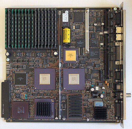
CPU キャッシュの初期の例としては、 1960 年代のAtlas 2 [ 3 ]やIBM System/360 Model 85 [ 4 ] [ 5 ]が挙げられます。キャッシュを使用した最初の CPU は、キャッシュが 1 レベルのみでした。後のレベル 1 キャッシュとは異なり、L1d (データ用) と L1i (命令用) に分割されていませんでした。分割 L1 キャッシュは 1976 年にIBM 801 CPU [ 6 ] [ 7 ]で始まり、1980 年代後半に主流となり、1997 年に ARMv5TE で組み込み CPU 市場に参入しました。2015 年現在、1ドル以下のSoCでさえL1 キャッシュを分割しています。また、L2 キャッシュも備えており、より大規模なプロセッサでは L3 キャッシュも備えています。L2 キャッシュは通常分割されておらず、既に分割されている L1 キャッシュの共通リポジトリとして機能します。マルチコア プロセッサの各コアには専用の L1 キャッシュがあり、通常はコア間で共有されません。 L2 キャッシュおよびそれより下位のキャッシュは、コア間で共有される場合があります。L4 キャッシュは現在では一般的ではなく、通常は静的ランダムアクセスメモリ(SRAM) ではなく、別のダイまたはチップ上の動的ランダムアクセスメモリ(DRAM) です。例外として、 L1 までのすべてのレベルのキャッシュにeDRAM が使用される場合があります。歴史的には、L1 も別のダイ上にありましたが、ダイサイズが大きくなったことで、最後のレベルを除いて、他のキャッシュレベルとともに統合できるようになりました。キャッシュの各レベルは、下位レベルよりも小さく、高速になる傾向があります。[ 8 ]
キャッシュ (歴史的に RAM と同様) は、一般的に 2、4、8、16 などのKiBのべき乗でサイズが決められてきました。MiBサイズ (つまり、より大きな非 L1 の場合)になると、非常に早い段階でこのパターンは崩れ、サイズを倍増させるパラダイムに強制されることなく、より大きなキャッシュを許容できるようになりました。たとえば、 2008 年 4 月に3 MiB の L2 キャッシュを備えたIntel Core 2 Duo が 登場しました。L1 キャッシュについては、そのサイズが一般的にまだ KiB の小さな数であるため、これはずっと後に起こりました。ただし、2012 年のIBM zEC12 は例外で、 当時としては異例に大きな 96 KiB の L1 データ キャッシュを獲得しました。たとえば、IBM z13は 96 KiB の L1 命令キャッシュ (および 128 KiB の L1 データ キャッシュ) を持ち、[ 9 ] 2018 年のIntel Ice Lake ベースのプロセッサは 48 KiB の L1 データ キャッシュと 48 KiB の L1 命令キャッシュを持っています 。 2020年、一部のIntel Atom CPU(最大24コア)は、4.5 MiBと15 MiBのキャッシュサイズ(またはその倍数)を備えています。[ 10 ] [ 11 ]
データは、キャッシュラインまたはキャッシュブロックと呼ばれる固定サイズのブロック単位でメモリとキャッシュ間で転送されます。キャッシュラインがメモリからキャッシュにコピーされると、キャッシュエントリが作成されます。キャッシュエントリには、コピーされたデータと要求されたメモリ位置(タグと呼ばれる)が含まれます。
プロセッサがメモリ内の特定の場所を読み書きする必要がある場合、まずキャッシュ内で対応するエントリを確認します。キャッシュは、要求されたメモリ位置の内容が、そのアドレスを含む可能性のあるすべてのキャッシュラインに存在するかどうかを確認します。プロセッサがメモリ位置がキャッシュ内に存在することを発見した場合、キャッシュヒットが発生したことになります。しかし、プロセッサがキャッシュ内にメモリ位置を見つけられなかった場合、キャッシュミスが発生したことになります。キャッシュヒットの場合、プロセッサは直ちにキャッシュライン内のデータを読み書きします。キャッシュミスの場合、キャッシュは新しいエントリを割り当て、メインメモリからデータをコピーし、その後、キャッシュの内容から要求を満たします。
キャッシュミス時に新しいエントリのためのスペースを確保するため、キャッシュは既存のエントリのいずれかを削除する必要がある場合があります。削除するエントリを選択するために使用するヒューリスティックは、置換ポリシーと呼ばれます。置換ポリシーの根本的な問題は、既存のキャッシュエントリのうち、将来使用される可能性が最も低いエントリを予測する必要があることです。将来を予測することは一般的に難しいため、利用可能なさまざまな置換ポリシーの中から最適なものを選ぶ完璧な方法はありません。よく使われる置換ポリシーの1つであるLRU( Least-Rested Used)は、最も最近アクセスされていないエントリを置き換えます。
一部のメモリ範囲をキャッシュ不可としてマークすることで、再アクセス頻度の低いメモリ領域のキャッシュを回避し、パフォーマンスを向上させることができます。これにより、再利用されないデータをキャッシュにロードする際のオーバーヘッドを回避できます。また、状況によっては、キャッシュエントリを無効化またはロックすることも可能です。
データがキャッシュに書き込まれると、いずれかの時点でメインメモリにも書き込まれる必要があります。この書き込みのタイミングは、書き込みポリシーと呼ばれます。ライトスルーキャッシュでは、キャッシュへの書き込みごとにメインメモリへの書き込みが発生します。一方、ライトバックキャッシュまたはコピーバックキャッシュでは、書き込みはすぐにメインメモリに反映されず、上書きされた場所はダーティとしてマークされ、キャッシュから追い出されたときにのみメインメモリに書き戻されます。このため、ライトバックキャッシュでの読み取りミスは、処理に2回のメモリアクセスが必要になる場合があります。1回目はダーティな場所をメインメモリに書き込むため、2回目はメモリから新しい場所を読み取るためです。また、ライトバックキャッシュにまだマッピングされていないメインメモリの場所への書き込みは、既にダーティになっている場所を追い出し、新しいメモリ場所のためにそのキャッシュ領域を解放する可能性があります。
中間的なポリシーも存在します。キャッシュはライトスルー方式ですが、書き込みデータは一時的にストアデータキューに保持される場合があります。これは通常、複数のストア処理をまとめて行うためであり、バスのターンアラウンド時間を短縮し、バスの利用率を向上させることができます。
メインメモリからキャッシュされたデータは、他のエンティティ(例えば、ダイレクトメモリアクセス(DMA)を使用する周辺機器や、マルチコアプロセッサの別のコアなど)によって変更される場合があり、その場合、キャッシュ内のコピーが古くなったり、陳腐化したりする可能性があります。また、マルチプロセッサシステムにおいてCPUがキャッシュ内のデータを更新すると、他のCPUに関連付けられたキャッシュ内のデータコピーが陳腐化します。データの一貫性を維持するためのキャッシュマネージャ間の通信プロトコルは、キャッシュコヒーレンスプロトコルと呼ばれます。
近年、メモリ性能とプロセッサ性能の速度差が指数関数的に拡大しているため、キャッシュ性能の測定が重要になってきています。キャッシュはこの速度差を縮小するために導入されました。そのため、特に高性能システムにおいては、キャッシュがプロセッサとメモリの速度差をどれだけ効果的に埋めることができるかを知ることが重要になります。キャッシュヒット率とキャッシュミス率は、この性能を決定する上で重要な役割を果たします。キャッシュ性能を向上させるには、ミス率を低減することが他の対策の中でも特に重要です。キャッシュへのアクセス時間を短縮することも、キャッシュ性能の向上につながり、最適化にも役立ちます。
The time taken to fetch one cache line from memory (read latency due to a cache miss) matters because the CPU will run out of work while waiting for the cache line. When a CPU reaches this state, it is called a stall. As CPUs become faster compared to main memory, stalls due to cache misses displace more potential computation; modern CPUs can execute hundreds of instructions in the time taken to fetch a single cache line from main memory.
Various techniques have been employed to keep the CPU busy during this time, including out-of-order execution in which the CPU attempts to execute independent instructions after the instruction that is waiting for the cache miss data. Another technology, used by many processors, is simultaneous multithreading (SMT), which allows an alternate thread to use the CPU core while the first thread waits for required CPU resources to become available.
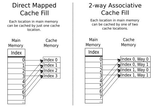
The placement policy decides where in the cache a copy of a particular entry of main memory will go. If the placement policy is free to choose any entry in the cache to hold the copy, the cache is called fully associative. At the other extreme, if each entry in the main memory can go in just one place in the cache, the cache is direct-mapped. Many caches implement a compromise in which each entry in the main memory can go to any one of N places in the cache, and are described as N-way set associative.[12] For example, the level-1 data cache in an AMD Athlon is two-way set associative, which means that any particular location in main memory can be cached in either of two locations in the level-1 data cache.
適切なアソシアティビティ値を選択するにはトレードオフが伴います。配置ポリシーによってメモリ位置をマッピングできる場所が10箇所ある場合、その位置がキャッシュにあるかどうかを確認するには、10個のキャッシュエントリを検索する必要があります。チェックする場所が増えると、消費電力とチップ面積が増え、時間も長くなる可能性があります。一方、アソシアティビティが高いキャッシュではミスが少なくなるため(競合ミスを参照)、CPUは低速なメインメモリからの読み出しに費やす時間を少なくすることができます。一般的なガイドラインとしては、アソシアティビティをダイレクトマップから2ウェイ、または2ウェイから4ウェイに倍増すると、ヒット率の向上効果はキャッシュサイズを倍増するのとほぼ同じです。ただし、アソシアティビティを4以上に増やしてもヒット率はそれほど向上せず[ 13 ]、通常は他の理由で行われます(仮想エイリアシングを参照)。一部のCPUは、低電力状態でキャッシュのアソシアティビティを動的に減らすことができ、これは省電力対策として機能します[ 14 ] 。
単純だが劣る順から、複雑だが優れている順に:
このキャッシュ構成では、メインメモリの各場所はキャッシュのエントリに 1 つだけ格納できます。そのため、ダイレクトマップ キャッシュは「一方向セット アソシアティブ」キャッシュとも呼ばれます。どのキャッシュ エントリの内容を追い出すかを選択できないため、配置ポリシーというものは存在しません。つまり、2 つの場所が同じエントリにマッピングされている場合、互いに追い出し合う可能性があります。ダイレクトマップ キャッシュは単純ですが、同等のパフォーマンスを得るにはアソシアティブ キャッシュよりもはるかに大きくする必要があり、予測不可能です。x をキャッシュ内のブロック番号、y をメモリのブロック番号、nをキャッシュ内のブロック数とすると、マッピングは方程式x = y mod nを使用して行われます。
メインメモリの各位置をキャッシュ内の2つの位置のいずれかにキャッシュできる場合、論理的な疑問は、どちらの位置を使用するかということです。最も単純で一般的に使用されている方式は、上の右側の図に示すように、メモリ位置のインデックスの最下位ビットをキャッシュメモリのインデックスとして使用し、各インデックスに対して2つのエントリを用意することです。この方式の利点の1つは、キャッシュに格納されるタグに、キャッシュメモリのインデックスによって示されるメインメモリアドレスの一部を含める必要がないことです。キャッシュタグのビット数が少ないため、必要なトランジスタ数が少なく、プロセッサ回路基板またはマイクロプロセッサチップ上のスペースを節約でき、読み取りと比較が高速になります。また、各ペアに対して1ビットだけを格納すればよいため、LRUアルゴリズムは特に単純です。
ダイレクトマップキャッシュの利点の1つは、シンプルかつ高速な投機実行が可能であることです。アドレスが計算されると、メモリ内のその場所のコピーが存在する可能性のあるキャッシュインデックスが1つ特定されます。そのキャッシュエントリを読み取ることができ、プロセッサはタグが要求されたアドレスと実際に一致するかどうかのチェックが完了する前に、そのデータを使って処理を続けることができます。
タグの一致が完了する前にプロセッサがキャッシュされたデータを使用するという考え方は、連想キャッシュにも適用できます。ヒントと呼ばれるタグのサブセットを使用して、要求されたアドレスにマッピングされる可能性のあるキャッシュエントリのうち、1つだけを選択できます。ヒントによって選択されたエントリは、完全なタグのチェックと並行して使用できます。ヒントの手法は、後述するように、アドレス変換のコンテキストで使用すると最も効果的です。
スキューキャッシュ[ 15 ]などの他の方式も提案されている。スキューキャッシュでは、ウェイ0のインデックスは上記のように直接だが、ウェイ1のインデックスはハッシュ関数で生成される。優れたハッシュ関数は、直接マッピングと競合するアドレスがハッシュ関数でマッピングされたときに競合しないという特性を持ち、そのため、病的なアクセスパターンによってプログラムが予期せず多数の競合ミスに悩まされる可能性が低くなる。欠点は、ハッシュ関数の計算による余分なレイテンシである。[ 16 ]さらに、新しいラインをロードして古いラインを追い出すとき、新しいラインが各ウェイの異なるインデックスのデータと競合するため、どの既存のラインが最も最近使用されていないかを判断するのが難しい場合がある。非スキューキャッシュのLRUトラッキングは通常、セット単位で行われる。それでも、スキューアソシアティブキャッシュは、従来のセットアソシアティブキャッシュに比べて大きな利点がある。[ 17 ]
真のセットアソシアティブキャッシュは、コンテンツアドレス指定可能なメモリなどを用いて、考えられるすべての方法を同時にテストします。擬似アソシアティブキャッシュは、考えられる各方法を一度に1つずつテストします。ハッシュリハッシュキャッシュとカラムアソシアティブキャッシュは、擬似アソシアティブキャッシュの例です。
最初にテストした方法でヒットが見つかった一般的なケースでは、擬似連想キャッシュは直接マップキャッシュと同じくらい高速ですが、直接マップキャッシュよりも競合ミス率がはるかに低く、完全連想キャッシュのミス率に近くなります。[ 16 ]
直接マップされたキャッシュと比較すると、セットアソシアティブキャッシュは、キャッシュセットにマッピングされるキャッシュセットインデックスのビット数が少なく、複数のウェイまたはブロックが残ります。たとえば、2ウェイセットアソシアティブキャッシュでは2ブロック、4ウェイセットアソシアティブキャッシュでは4ブロックです。直接マップされたキャッシュと比較すると、未使用のキャッシュインデックスビットはタグビットの一部になります。たとえば、2ウェイセットアソシアティブキャッシュはタグに1ビットを提供し、4ウェイセットアソシアティブキャッシュはタグに2ビットを提供します。マルチカラムキャッシュ[ 18 ]の基本的な考え方は、従来のセットアソシアティブキャッシュと同様にセットインデックスを使用してキャッシュセットにマッピングし、追加されたタグビットを使用してセット内のウェイをインデックスすることです。たとえば、4ウェイセットアソシアティブキャッシュでは、2ビットはそれぞれウェイ00、ウェイ01、ウェイ10、ウェイ11をインデックスするために使用されます。この二重キャッシュインデックスは「メジャーロケーションマッピング」と呼ばれ、そのレイテンシはダイレクトマップアクセスと同等です。マルチカラムキャッシュ設計[ 18 ]の広範な実験では、メジャーロケーションへのヒット率が90%にも達することが示されています。キャッシュマッピングがメジャーロケーションのキャッシュブロックと競合する場合、既存のキャッシュブロックは同じセット内の別のキャッシュウェイに移動され、これを「選択ロケーション」と呼びます。新しくインデックス付けされたキャッシュブロックは最近使用された(MRU)ブロックであるため、時間的局所性を考慮してマルチカラムキャッシュのメジャーロケーションに配置されます。マルチカラムキャッシュは高い連想性を持つキャッシュ用に設計されているため、各セットのウェイ数が多く、セット内の選択ロケーションを簡単に見つけることができます。キャッシュブロック内のメジャーロケーションについては、追加のハードウェアによって選択ロケーションインデックスが維持されます。
Multicolumn cache remains a high hit ratio due to its high associativity, and has a comparable low latency to a direct-mapped cache due to its high percentage of hits in major locations. The concepts of major locations and selected locations in multicolumn cache have been used in several cache designs in ARM Cortex R chip,[19] Intel's way-predicting cache memory,[20] IBM's reconfigurable multi-way associative cache memory[21] and Oracle's dynamic cache replacement way selection based on address tab bits.[22]
Cache row entries usually have the following structure:
The data block (cache line) contains the actual data fetched from the main memory. The tag contains (part of) the address of the actual data fetched from the main memory. The flag bits are discussed below.
The "size" of the cache is the amount of main memory data it can hold. This size can be calculated as the number of bytes stored in each data block times the number of blocks stored in the cache. (The tag, flag and error correction code bits are not included in the size,[23] although they do affect the physical area of a cache.)
An effective memory address which goes along with the cache line (memory block) is split (MSB to LSB) into the tag, the index and the block offset.[8][24]
The index describes which cache set that the data has been put in. The index length is bits for s cache sets.
The block offset specifies the desired data within the stored data block within the cache row. Typically the effective address is in bytes, so the block offset length is bits, where b is the number of bytes per data block. The tag contains the most significant bits of the address, which are checked against all rows in the current set (the set has been retrieved by index) to see if this set contains the requested address. If it does, a cache hit occurs. The tag length in bits is as follows:
tag_length = address_length - index_length - block_offset_lengthSome authors refer to the block offset as simply the "offset"[25] or the "displacement".[26][27]
オリジナルのPentium 4プロセッサは、8 KiBサイズの 4 ウェイ セット アソシアティブ L1 データ キャッシュを備えており、キャッシュ ブロックは 64 バイトでした。したがって、キャッシュ ブロックは 8 KiB / 64 = 128 個あります。セットの数は、キャッシュ ブロックの数をアソシアティビティのウェイの数で割った値に等しく、128 / 4 = 32 セットとなり、2 5 = 32 種類のインデックスが存在します。オフセットは 2 6 = 64通りあります。CPU アドレスは 32 ビット幅であるため、タグ フィールドには32 − 5 − 6 = 21 ビットが使用されることになります。
オリジナルの Pentium 4 プロセッサには、128 バイトのキャッシュ ブロックを持つ 256 KiB の 8 ウェイ セット アソシアティブ L2 統合キャッシュも搭載されていました。これは、タグ フィールドが32 − 8 − 7 = 17 ビット であることを意味します。 [ 25 ]
命令キャッシュは、キャッシュ行エントリごとに1つのフラグビット(有効ビット)のみを必要とします。有効ビットは、キャッシュブロックに有効なデータがロードされているかどうかを示します。
電源投入時、ハードウェアはすべてのキャッシュ内の有効なビットをすべて「無効」に設定します。システムによっては、マルチマスターバススヌーピングハードウェアが、あるプロセッサのキャッシュ内で他のプロセッサからブロードキャストされたアドレスを受信し、ローカルキャッシュ内の特定のデータブロックが古くなっていることを認識して無効としてマークする必要がある場合など、他のタイミングで有効なビットを「無効」に設定することもあります。
データキャッシュは通常、キャッシュラインごとに2つのフラグビット(有効ビットとダーティビット)を必要とします。ダーティビットがセットされているということは、メインメモリから読み出された後、関連するキャッシュラインが変更された(「ダーティ」)ことを示します。つまり、プロセッサがそのラインにデータを書き込みましたが、新しい値がメインメモリまで完全に伝播していないことを意味します。
キャッシュミスとは、キャッシュ内のデータの読み書きに失敗した状態を指し、その結果、メインメモリへのアクセスが大幅に遅延します。キャッシュミスには、命令読み取りミス、データ読み取りミス、データ書き込みミスの3種類があります。
Cache read misses from an instruction cache generally cause the largest delay, because the processor, or at least the thread of execution, has to wait (stall) until the instruction is fetched from main memory. Cache read misses from a data cache usually cause a smaller delay, because instructions not dependent on the cache read can be issued and continue execution until the data are returned from main memory, and the dependent instructions can resume execution. Cache write misses to a data cache generally cause the shortest delay, because the write can be queued and there are few limitations on the execution of subsequent instructions; the processor can continue until the queue is full. For a detailed introduction to the types of misses, see cache performance measurement and metric.
Most general purpose CPUs implement some form of virtual memory. To summarize, either each program running on the machine sees its own simplified address space, which contains code and data for that program only, or all programs run in a common virtual address space. A program executes by calculating, comparing, reading and writing to addresses of its virtual address space, rather than addresses of physical address space, making programs simpler and thus easier to write.
Virtual memory requires the processor to translate virtual addresses generated by the program into physical addresses in main memory. The portion of the processor that does this translation is known as the memory management unit (MMU). The fast path through the MMU can perform those translations stored in the translation lookaside buffer (TLB), which is a cache of mappings from the operating system's page table, segment table, or both.
For the purposes of the present discussion, there are three important features of address translation:
One early virtual memory system, the IBM M44/44X, required an access to a mapping table held in core memory before every programmed access to main memory.[28][NB 1] With no caches, and with the mapping table memory running at the same speed as main memory this effectively cut the speed of memory access in half. Two early machines that used a page table in main memory for mapping, the IBM System/360 Model 67 and the GE 645, both had a small associative memory as a cache for accesses to the in-memory page table. Both machines predated the first machine with a cache for main memory, the IBM System/360 Model 85, so the first hardware cache used in a computer system was not a data or instruction cache, but rather a TLB.
Caches can be divided into four types, based on whether the index or tag correspond to physical or virtual addresses:
The speed of this recurrence (the load latency) is crucial to CPU performance, and so most modern level-1 caches are virtually indexed, which at least allows the MMU's TLB lookup to proceed in parallel with fetching the data from the cache RAM.
But virtual indexing is not the best choice for all cache levels. The cost of dealing with virtual aliases grows with cache size, and as a result most level-2 and larger caches are physically indexed.
Caches have historically used both virtual and physical addresses for the cache tags, although virtual tagging is now uncommon. If the TLB lookup can finish before the cache RAM lookup, then the physical address is available in time for tag compare, and there is no need for virtual tagging. Large caches, then, tend to be physically tagged, and only small, very low latency caches are virtually tagged. In recent general-purpose CPUs, virtual tagging has been superseded by virtual hints, as described below.
A cache that relies on virtual indexing and tagging becomes inconsistent after the same virtual address is mapped into different physical addresses (homonym), which can be solved by using physical address for tagging, or by storing the address space identifier in the cache line. However, the latter approach does not help against the synonym problem, in which several cache lines end up storing data for the same physical address. Writing to such locations may update only one location in the cache, leaving the others with inconsistent data. This issue may be solved by using non-overlapping memory layouts for different address spaces, or otherwise the cache (or a part of it) must be flushed when the mapping changes.[34]
仮想タグの大きな利点は、連想キャッシュの場合、仮想アドレスから物理アドレスへの変換が行われる前にタグの一致処理を進めることができる点です。しかし、コヒーレンスプローブや削除処理では、処理対象の物理アドレスが提示されます。ハードウェアは、物理アドレスをキャッシュインデックスに変換する何らかの手段を備えている必要があり、通常は仮想タグだけでなく物理タグも格納します。比較のために述べると、物理タグ付きキャッシュは仮想タグを保持する必要がないため、よりシンプルです。TLBから仮想アドレスから物理アドレスへのマッピングが削除されると、その仮想アドレスを持つキャッシュエントリは、何らかの方法でフラッシュする必要があります。あるいは、TLBによってマッピングされていないページにキャッシュエントリが許可されている場合、ページテーブルでそれらのページのアクセス権が変更されると、それらのエントリはフラッシュする必要があります。
オペレーティングシステムは、仮想エイリアスがキャッシュ内に同時に存在しないことを保証することも可能です。オペレーティングシステムは、後述するページカラーリングを強制することでこの保証を実現します。初期のRISCプロセッサ(SPARC、RS/6000など)の中には、この方式を採用していたものもありました。しかし、仮想エイリアスの検出と削除にかかるハードウェアコストが低下し、完全なページカラーリングによるソフトウェアの複雑さとパフォーマンスの低下が増大したため、近年ではこの方式は使用されなくなりました。
連想キャッシュにおけるタグの2つの機能を区別することは有用である。タグはエントリセットのどの方向を選択するかを決定するために使用され、キャッシュがヒットしたかミスしたかを決定するために使用される。2番目の機能は常に正しくなければならないが、1番目の機能は推測に基づいて、時折間違った結果を出すことが許容される。
一部のプロセッサ(初期のSPARCなど)は、仮想タグと物理タグの両方を持つキャッシュを備えています。仮想タグはウェイ選択に使用され、物理タグはヒットかミスかを判定するために使用されます。このタイプのキャッシュは、仮想タグ付きキャッシュの低遅延性と、物理タグ付きキャッシュのシンプルなソフトウェアインターフェースという利点を享受できます。ただし、タグが重複するというコストが加わります。また、ミス処理時には、インデックス付けされたキャッシュラインの代替ウェイをプローブして仮想エイリアスを探し、一致するものがあれば削除する必要があります。
仮想タグの代わりに仮想ヒントを各キャッシュエントリに保持することで、余分な領域(および若干の遅延)を軽減できます。これらのヒントは仮想タグのサブセットまたはハッシュであり、キャッシュからデータと物理タグを取得する方法を選択するために使用されます。仮想タグ付きキャッシュと同様に、仮想ヒントが一致しても物理タグが一致しない場合があり、その場合は一致するヒントを持つキャッシュエントリを削除して、このアドレスのキャッシュが満たされた後のキャッシュアクセスで一致するヒントが1つだけになるようにする必要があります。仮想ヒントは仮想タグよりもビット数が少ないため、仮想ヒント付きキャッシュは仮想タグ付きキャッシュよりも競合ミスが多くなります。
Perhaps the ultimate reduction of virtual hints can be found in the Pentium 4 (Willamette and Northwood cores). In these processors the virtual hint is effectively two bits, and the cache is four-way set associative. Effectively, the hardware maintains a simple permutation from virtual address to cache index, so that no content-addressable memory (CAM) is necessary to select the right one of the four ways fetched.
Large physically indexed caches (usually secondary caches) run into a problem: the operating system rather than the application controls which pages collide with one another in the cache. Differences in page allocation from one program run to the next lead to differences in the cache collision patterns, which can lead to very large differences in program performance. These differences can make it very difficult to get a consistent and repeatable timing for a benchmark run.
To understand the problem, consider a CPU with a 1 MiB physically indexed direct-mapped level-2 cache and 4 KiB virtual memory pages. Sequential physical pages map to sequential locations in the cache until after 256 pages the pattern wraps around. We can label each physical page with a color of 0–255 to denote where in the cache it can go. Locations within physical pages with different colors cannot conflict in the cache.
Programmers attempting to make maximum use of the cache may arrange their programs' access patterns so that only 1 MiB of data need be cached at any given time, thus avoiding capacity misses. But they should also ensure that the access patterns do not have conflict misses. One way to think about this problem is to divide up the virtual pages the program uses and assign them virtual colors in the same way as physical colors were assigned to physical pages before. Programmers can then arrange the access patterns of their code so that no two pages with the same virtual color are in use at the same time. There is a wide literature on such optimizations (e.g. loop nest optimization), largely coming from the High Performance Computing (HPC) community.
The snag is that while all the pages in use at any given moment may have different virtual colors, some may have the same physical colors. In fact, if the operating system assigns physical pages to virtual pages randomly and uniformly, it is extremely likely that some pages will have the same physical color, and then locations from those pages will collide in the cache (this is the birthday paradox).
The solution is to have the operating system attempt to assign different physical color pages to different virtual colors, a technique called page coloring. Although the actual mapping from virtual to physical color is irrelevant to system performance, odd mappings are difficult to keep track of and have little benefit, so most approaches to page coloring simply try to keep physical and virtual page colors the same.
If the operating system can guarantee that each physical page maps to only one virtual color, then there are no virtual aliases, and the processor can use virtually indexed caches with no need for extra virtual alias probes during miss handling. Alternatively, the OS can flush a page from the cache whenever it changes from one virtual color to another. As mentioned above, this approach was used for some early SPARC and RS/6000 designs.
The software page coloring technique has been used to effectively partition the shared Last level Cache (LLC) in multicore processors.[35] This operating system-based LLC management in multicore processors has been adopted by Intel.[36]

Modern processors have multiple interacting on-chip caches. The operation of a particular cache can be completely specified by the cache size, the cache block size, the number of blocks in a set, the cache set replacement policy, and the cache write policy (write-through or write-back).[25]
While all of the cache blocks in a particular cache are the same size and have the same associativity, typically the "higher-level" caches (called Level 1 cache) have a smaller number of blocks, smaller block size, and fewer blocks in a set, but have very short access times. "Lower-level" caches (i.e. Level 2 and below) have progressively larger numbers of blocks, larger block size, more blocks in a set, and relatively longer access times, but are still much faster than main memory.[8]
Cache entry replacement policy is determined by a cache algorithm selected to be implemented by the processor designers. In some cases, multiple algorithms are provided for different kinds of work loads.
パイプライン型CPUは、命令フェッチ、仮想アドレスから物理アドレスへの変換、データフェッチといったパイプライン内の複数のポイントからメモリにアクセスします(従来のRISCパイプラインを参照)。これらのポイントごとに異なる物理キャッシュを使用するのが自然な設計であり、1つの物理リソースをパイプライン内の2つのポイントに割り当てて処理する必要がなくなります。そのため、パイプラインは必然的に少なくとも3つの独立したキャッシュ(命令キャッシュ、TLBキャッシュ、データキャッシュ)を持つようになり、それぞれが特定の役割に特化しています。
ビクティムキャッシュは、CPU キャッシュの交換時に追い出されたブロックを保持するために使用されるキャッシュです。ビクティム キャッシュはメイン キャッシュとその補充パスの間に位置し、メイン キャッシュから追い出されたデータ ブロックのみを保持します。ビクティム キャッシュは通常、完全な連想性を持ち、競合ミスの数を減らすことを目的としています。一般的に使用される多くのプログラムでは、すべてのアクセスに対して連想マッピングは必要ありません。実際、プログラムのメモリ アクセスのごく一部だけが、高い連想性を必要とします。ビクティム キャッシュはこの特性を利用して、これらのアクセスのみに高い連想性を提供します。これは、1990 年に DEC のNorman Jouppiによって導入されました。 [ 37 ]
IntelのHaswellプロセッサのCrystalwell [ 38 ]バリアントでは、プロセッサのレベル3キャッシュのビクティムキャッシュとして機能する、パッケージ上の128 MiB eDRAMレベル4キャッシュが導入されました。 [ 39 ] Skylakeマイクロアーキテクチャでは、レベル4キャッシュはビクティムキャッシュとして機能しなくなりました。[ 40 ]
キャッシュ特化の極端な例の 1 つは、Intel Pentium 4マイクロプロセッサに搭載されているトレース キャッシュ(実行トレース キャッシュとも呼ばれる) です。トレース キャッシュは、既にフェッチおよびデコードされた命令のトレースを保存することで、命令フェッチ帯域幅を増やし、消費電力 (Pentium 4 の場合)を削減するメカニズムです。[ 41 ]
トレースキャッシュは、命令がデコードされた後、または実行が終了した後に命令を格納します。一般的に、命令は個々の基本ブロックまたは動的命令トレースを表すグループとしてトレースキャッシュに追加されます。Pentium 4のトレースキャッシュは、x86命令のデコードによって生成されたマイクロオペレーションを格納し、マイクロオペレーションキャッシュの機能も提供します。これにより、次に命令が必要になったときに、マイクロオペレーションに再度デコードする必要がなくなります。[ 42 ] : 63-68
ライトコアレッシングキャッシュ[ 43 ]は、 AMDのBulldozerマイクロアーキテクチャのL2キャッシュの一部である特殊なキャッシュです。モジュール内の両方のL1DキャッシュからのストアはWCCを経由し、そこでバッファリングおよびコアレッシングされます。WCCの役割は、L2キャッシュへの書き込み回数を減らすことです。
マイクロオペレーションキャッシュ(μopキャッシュ、uopキャッシュ、またはUC)[ 44 ]は、命令デコーダまたは命令キャッシュから直接受け取った、デコードされた命令のマイクロオペレーションを格納する特殊なキャッシュです。命令をデコードする必要がある場合、μopキャッシュがチェックされ、デコードされた形式がキャッシュされている場合は再利用されます。利用できない場合は、命令がデコードされてからキャッシュされます。
Intel P6 プロセッサ ファミリーの代替フロントエンドとして μop キャッシュを説明した初期の研究の 1 つは、2001 年の論文「Micro-Operation Cache: A Power Aware Frontend for Variable Instruction Length ISA」です。[ 45 ]その後、Intel は、 Sandy Bridgeプロセッサや、 Ivy BridgeやHaswellなどの後継のマイクロ アーキテクチャにμop キャッシュを組み込みました。[ 42 ] : 121–123 [ 46 ] AMD は、 Zen マイクロ アーキテクチャに μop キャッシュを実装しました。[ 47 ]
Fetching complete pre-decoded instructions eliminates the need to repeatedly decode variable length complex instructions into simpler fixed-length micro-operations, and simplifies the process of predicting, fetching, rotating and aligning fetched instructions. A μop cache effectively offloads the fetch and decode hardware, thus decreasing power consumption and improving the frontend supply of decoded micro-operations. The μop cache also increases performance by more consistently delivering decoded micro-operations to the backend and eliminating various bottlenecks in the CPU's fetch and decode logic.[45][46]
A μop cache has many similarities with a trace cache, although a μop cache is much simpler thus providing better power efficiency; this makes it better suited for implementations on battery-powered devices. The main disadvantage of the trace cache, leading to its power inefficiency, is the hardware complexity required for its heuristic deciding on caching and reusing dynamically created instruction traces.[48]
A branch target cache or branch target instruction cache, the name used on ARM microprocessors,[49] is a specialized cache which holds the first few instructions at the destination of a taken branch. This is used by low-powered processors which do not need a normal instruction cache because the memory system is capable of delivering instructions fast enough to satisfy the CPU without one. However, this only applies to consecutive instructions in sequence; it still takes several cycles of latency to restart instruction fetch at a new address, causing a few cycles of pipeline bubble after a control transfer. A branch target cache provides instructions for those few cycles avoiding a delay after most taken branches.
This allows full-speed operation with a much smaller cache than a traditional full-time instruction cache.
Smart cache is a level 2 or level 3 caching method for multiple execution cores, developed by Intel.
Smart Cache shares the actual cache memory between the cores of a multi-core processor. In comparison to a dedicated per-core cache, the overall cache miss rate decreases when cores do not require equal parts of the cache space. Consequently, a single core can use the full level 2 or level 3 cache while the other cores are inactive.[50] Furthermore, the shared cache makes it faster to share memory among different execution cores.[51]
Another issue is the fundamental tradeoff between cache latency and hit rate. Larger caches have better hit rates but longer latency. To address this tradeoff, many computers use multiple levels of cache, with small fast caches backed up by larger, slower caches. Multi-level caches generally operate by checking the fastest but smallest cache, level 1 (L1), first; if it hits, the processor proceeds at high speed. If that cache misses, the slower but larger next level cache, level 2 (L2), is checked, and so on, before accessing external memory.
As the latency difference between main memory and the fastest cache has become larger, some processors have begun to utilize as many as three levels of on-chip cache. Price-sensitive designs used this to pull the entire cache hierarchy on-chip, but by the 2010s some of the highest-performance designs returned to having large off-chip caches, which is often implemented in eDRAM and mounted on a multi-chip module, as a fourth cache level. In rare cases, such as in the mainframe CPU IBM z15 (2019), all levels down to L1 are implemented by eDRAM, replacing SRAM entirely (for cache, SRAM is still used for registers). Apple'sARM-basedApple silicon series, starting with the A14 and M1, have a 192 KiB L1i cache for each of the high-performance cores, an unusually large amount; however the high-efficiency cores only have 128 KiB. Since then other processors such as Intel's Lunar Lake and Qualcomm's Oryon have also implemented similar L1i cache sizes.
The benefits of L3 and L4 caches depend on the application's access patterns. Examples of products incorporating L3 and L4 caches include the following:
Finally, at the other end of the memory hierarchy, the CPU register file itself can be considered the smallest, fastest cache in the system, with the special characteristic that it is scheduled in software—typically by a compiler, as it allocates registers to hold values retrieved from main memory for, as an example, loop nest optimization. However, with register renaming most compiler register assignments are reallocated dynamically by hardware at runtime into a register bank, allowing the CPU to break false data dependencies and thus easing pipeline hazards.
Register files sometimes also have hierarchy: The Cray-1 (circa 1976) had eight address "A" and eight scalar data "S" registers that were generally usable. There was also a set of 64 address "B" and 64 scalar data "T" registers that took longer to access, but were faster than main memory. The "B" and "T" registers were provided because the Cray-1 did not have a data cache. (The Cray-1 did, however, have an instruction cache.)
When considering a chip with multiple cores, there is a question of whether the caches should be shared or local to each core. Implementing shared cache inevitably introduces more wiring and complexity. But then, having one cache per chip, rather than core, greatly reduces the amount of space needed, and thus one can include a larger cache.
Typically, sharing the L1 cache is undesirable because the resulting increase in latency would make each core run considerably slower than a single-core chip. However, for the highest-level cache (usually L3, the last one called before accessing memory), having a global cache is desirable for several reasons, such as allowing a single core to use the whole cache, reducing data redundancy by making it possible for different processes or threads to share cached data, and reducing the complexity of utilized cache coherency protocols.[53] For example, an eight-core chip with three levels may include an L1 cache for each core, one intermediate L2 cache for each pair of cores, and one L3 cache shared between all cores.
共有される最上位レベルのキャッシュ(通常はメモリにアクセスする前に呼び出されるL3)は、通常、最終レベルキャッシュ(LLC)と呼ばれます。[ 54 ] LLCが複数のコア間で共有される場合、並列性を高めるための追加の手法が使用されます。これには、LLCを特定のメモリ アドレス範囲をアドレス指定し、独立してアクセスできる複数の断片にスライスすることが含まれます。[ 8 ] [ 55 ]
独立したキャッシュ構造では、命令とデータは別々にキャッシュされるため、キャッシュラインは命令またはデータのいずれかをキャッシュするために使用され、両方をキャッシュするためには使用されません。データと命令の変換ルックアサイドバッファを分離することで、さまざまな利点が実証されています。[ 56 ]統合構造では、この制約はなく、キャッシュラインを使用して命令とデータの両方をキャッシュできます。
マルチレベルキャッシュは、新たな設計上の決定事項をもたらします。たとえば、一部のプロセッサでは、L1 キャッシュ内のすべてのデータは、L2 キャッシュのどこかにも存在する必要があります。これらのキャッシュは、厳密に包含的と呼ばれます。他のプロセッサ ( AMD Athlonなど)は排他的キャッシュを備えています。データは、L1 キャッシュと L2 キャッシュのうち最大で 1 つに存在することが保証されており、両方に存在することはありません。さらに他のプロセッサ (Intel Pentium II、III、および4など) では、L1 キャッシュ内のデータが L2 キャッシュにも存在する必要はありませんが、多くの場合、存在する可能性があります。この中間的なポリシーには、普遍的に受け入れられている名前はありません。 [ 57 ] [ 58 ] 2 つの一般的な名前は、「非排他的」と「部分的に包含的」です。
排他キャッシュの利点は、より多くのデータを格納できることです。この利点は、排他L1キャッシュがL2キャッシュと同程度の場合に大きくなり、L2キャッシュがL1キャッシュより何倍も大きい場合は小さくなります。アクセス時にL1がミスし、L2がヒットした場合、L2のヒットしたキャッシュラインがL1のラインと交換されます。この交換は、インクルーシブキャッシュが行うように、L2からL1にラインをコピーするよりもかなり多くの作業が必要です。[ 58 ]
One advantage of strictly inclusive caches is that when external devices or other processors in a multiprocessor system wish to remove a cache line from the processor, they need only have the processor check the L2 cache. In cache hierarchies which do not enforce inclusion, the L1 cache must be checked as well. As a drawback, there is a correlation between the associativities of L1 and L2 caches: if the L2 cache does not have at least as many ways as all L1 caches together, the effective associativity of the L1 caches is restricted. Another disadvantage of inclusive cache is that whenever there is an eviction in L2 cache, the (possibly) corresponding lines in L1 also have to get evicted in order to maintain inclusiveness. This is quite a bit of work, and would result in a higher L1 miss rate.[58]
Another advantage of inclusive caches is that the larger cache can use larger cache lines, which reduces the size of the secondary cache tags. (Exclusive caches require both caches to have the same size cache lines, so that cache lines can be swapped on a L1 miss, L2 hit.) If the secondary cache is an order of magnitude larger than the primary, and the cache data are an order of magnitude larger than the cache tags, this tag area saved can be comparable to the incremental area needed to store the L1 cache data in the L2.[59]
Scratchpad memory (SPM), also known as scratchpad, scratchpad RAM or local store in computer terminology, is a high-speed internal memory used for temporary storage of calculations, data, and other work in progress.
To illustrate both specialization and multi-level caching, here is the cache hierarchy of the K8 core in the AMD Athlon 64 CPU.[60]
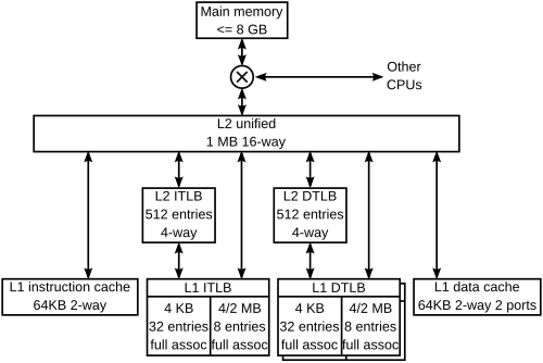
The K8 has four specialized caches: an instruction cache, an instruction TLB, a data TLB, and a data cache. Each of these caches is specialized:
The K8 also has multiple-level caches. There are second-level instruction and data TLBs, which store only PTEs mapping 4 KiB. Both instruction and data caches, and the various TLBs, can fill from the large unified L2 cache. This cache is exclusive to both the L1 instruction and data caches, which means that any 8-byte line can only be in one of the L1 instruction cache, the L1 data cache, or the L2 cache. It is, however, possible for a line in the data cache to have a PTE which is also in one of the TLBs—the operating system is responsible for keeping the TLBs coherent by flushing portions of them when the page tables in memory are updated.
The K8 also caches information that is never stored in memory—prediction information. These caches are not shown in the above diagram. As is usual for this class of CPU, the K8 has fairly complex branch prediction, with tables that help predict whether branches are taken and other tables which predict the targets of branches and jumps. Some of this information is associated with instructions, in both the level 1 instruction cache and the unified secondary cache.
K8は、二次キャッシュ内の命令に予測情報を格納するための興味深い手法を採用しています。二次キャッシュ内のラインは、データ一次キャッシュまたは命令一次キャッシュのどちらから追い出されたかに応じて、 ECCまたはパリティによって偶発的なデータ破損(例えば、アルファ粒子の衝突など)から保護されます。パリティコードはECCコードよりもビット数が少ないため、命令キャッシュからのラインには若干の余剰ビットが残ります。これらのビットは、当該命令に関連付けられた分岐予測情報をキャッシュするために使用されます。結果として、分岐予測器の実効履歴テーブルが大きくなり、精度が向上します。
他のプロセッサには、別の種類の予測器が搭載されています(例えば、 DEC Alpha 21264のストア・トゥ・ロード・バイパス予測器など)。
これらの予測器は、計算コストの高い情報を格納するという点でキャッシュの一種です。予測器について議論する際に用いられる用語の中には、キャッシュの用語と同じものもあります(例えば、分岐予測器におけるヒットなど)が、予測器は一般的にキャッシュ階層の一部とは考えられていません。
K8プロセッサは、命令キャッシュとデータキャッシュの一貫性をハードウェアで維持します。つまり、ストア命令の直後の命令にストア命令を実行すると、その直後の命令も変更されます。AlphaやMIPSファミリーなどの他のプロセッサは、命令キャッシュの一貫性を維持するためにソフトウェアに依存しています。ストア命令は、プログラムがオペレーティングシステムの機能を呼び出して一貫性を確保するまで、命令ストリームに反映されるとは限りません。

コンピュータ工学では、タグRAMを使用して、CPUキャッシュに現在格納されているメモリ位置を指定します。[ 61 ] [ 62 ]単純な直接マップ設計では、高速SRAMを使用できます。高次の連想キャッシュは通常、コンテンツアドレス指定可能なメモリを使用します。
キャッシュ読み出しは、1サイクル以上を要する最も一般的なCPU操作です。プログラムの実行時間は、レベル1データキャッシュヒットのレイテンシに非常に敏感です。そのため、キャッシュを可能な限り高速化するために、多大な設計労力、そして多くの場合、電力とシリコン面積が費やされます。
The simplest cache is a virtually indexed direct-mapped cache. The virtual address is calculated with an adder, the relevant portion of the address extracted and used to index an SRAM, which returns the loaded data. The data are byte aligned in a byte shifter, and from there are bypassed to the next operation. There is no need for any tag checking in the inner loop –in fact, the tags need not even be read. Later in the pipeline, but before the load instruction is retired, the tag for the loaded data must be read, and checked against the virtual address to make sure there was a cache hit. On a miss, the cache is updated with the requested cache line and the pipeline is restarted.
An associative cache is more complicated, because some form of tag must be read to determine which entry of the cache to select. An N-way set-associative level-1 cache usually reads all N possible tags and N data in parallel, and then chooses the data associated with the matching tag. Level-2 caches sometimes save power by reading the tags first, so that only one data element is read from the data SRAM.
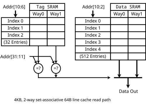
The adjacent diagram is intended to clarify the manner in which the various fields of the address are used. Address bit 31 is most significant, bit 0 is least significant. The diagram shows the SRAMs, indexing, and multiplexing for a 4 KiB, 2-way set-associative, virtually indexed and virtually tagged cache with 64 byte (B) lines, a 32-bit read width and 32-bit virtual address.
Because the cache is 4 KiB and has 64 B lines, there are just 64 lines in the cache, and we read two at a time from a Tag SRAM which has 32 rows, each with a pair of 21 bit tags. Although any function of virtual address bits 31 through 6 could be used to index the tag and data SRAMs, it is simplest to use the least significant bits.
Similarly, because the cache is 4 KiB and has a 4 B read path, and reads two ways for each access, the Data SRAM is 512 rows by 8 bytes wide.
A more modern cache might be 16 KiB, 4-way set-associative, virtually indexed, virtually hinted, and physically tagged, with 32 B lines, 32-bit read width and 36-bit physical addresses. The read path recurrence for such a cache looks very similar to the path above. Instead of tags, virtual hints are read, and matched against a subset of the virtual address. Later on in the pipeline, the virtual address is translated into a physical address by the TLB, and the physical tag is read (just one, as the virtual hint supplies which way of the cache to read). Finally the physical address is compared to the physical tag to determine if a hit has occurred.
Some SPARC designs have improved the speed of their L1 caches by a few gate delays by collapsing the virtual address adder into the SRAM decoders.
キャッシュ技術の初期の歴史は、仮想メモリの発明と利用に密接に関係しています。半導体メモリの希少性とコストのため、1960年代の初期のメインフレームコンピュータは、プログラムが使用するフラットな仮想メモリ空間にマッピングされた複雑な物理メモリ階層を使用していました。メモリ技術は、半導体、磁気コア、ドラム、ディスクに及びました。プログラムが認識し使用する仮想メモリはフラットであり、キャッシュを使用して、プロセッサがアクセスする前にデータと命令を最速のメモリにフェッチしました。キャッシュサイズを最適化するために広範な研究が行われました。最適な値は使用するプログラミング言語に大きく依存することがわかりました。Algolは最小のキャッシュサイズを必要とし、FortranとCobolは最大のキャッシュサイズを必要としました。
マイクロコンピュータ技術の初期の頃は、メモリへのアクセス速度はレジスタへのアクセス速度よりわずかに遅いだけでした。しかし、1980年代以降[ 63 ]、プロセッサとメモリの性能差は拡大してきました。マイクロプロセッサはメモリよりもはるかに速く進化しており、特に動作周波数の面で顕著です。そのため、メモリが性能のボトルネックとなりました。技術的にはメインメモリ全体をCPUと同じ速度にすることは可能でしたが、より経済的に実現可能な道が取られました。それは、低速メモリを大量に使用しつつ、性能差を緩和するために小型の高速キャッシュメモリを導入するというものです。これにより、同じ価格で桁違いに容量が増え、総合的な性能はわずかに低下するだけで済みました。
TLBの最初の使用例はGE 645 [ 64 ]とIBM 360/67 [ 65 ]で、どちらもTLBとして連想メモリを使用していた。
1982年に発売された68010は、「ループモード」と呼ばれる、わずか2つの命令で構成されるループ処理を高速化する、小型で特殊な命令キャッシュを備えていました。 1984年に発売された68020は、これを256バイトの標準的な命令キャッシュに置き換え、真のオンチップキャッシュメモリを搭載した最初の68kシリーズプロセッサとなりました。
1987年にリリースされた68030は、基本的に68020コアに256バイトのデータキャッシュ、オンチップメモリ管理ユニット(MMU)、プロセス縮小、およびキャッシュのバーストモードを追加したものです。
The 68040, released in 1990, has split instruction and data caches of four kilobytes each.
The 68060, released in 1994, has the following: 8 KiB data cache (four-way associative), 8 KiB instruction cache (four-way associative), 96-byte FIFO instruction buffer, 256-entry branch cache, and 64-entry address translation cache MMU buffer (four-way associative).
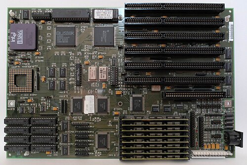
As the x86 microprocessors reached clock rates of 20 MHz and above in the 386, small amounts of fast cache memory began to be featured in systems to improve performance. This was because the DRAM used for main memory had significant latency, up to 120 ns, as well as refresh cycles. The cache was constructed from more expensive, but significantly faster, SRAMmemory cells, which at the time had latencies around 10–25 ns. The early caches were external to the processor and typically located on the motherboard in the form of eight or nine DIP devices placed in sockets to enable the cache as an optional extra or upgrade feature.
Some versions of the Intel 386 processor could support 16 to 256 KiB of external cache.
With the 486 processor, an 8 KiB cache was integrated directly into the CPU die. This cache was termed Level 1 or L1 cache to differentiate it from the slower on-motherboard, or Level 2 (L2) cache. These on-motherboard caches were much larger, with the most common size being 256 KiB. There were some system boards that contained sockets for the Intel 485Turbocache daughtercard which had either 64 or 128 Kbyte of cache memory.[68][69] The popularity of on-motherboard cache continued through the Pentium MMX era but was made obsolete by the introduction of SDRAM and the growing disparity between bus clock rates and CPU clock rates, which caused on-motherboard cache to be only slightly faster than main memory.
The next development in cache implementation in the x86 microprocessors began with the Pentium Pro, which brought the secondary cache onto the same package as the microprocessor, clocked at the same frequency as the microprocessor.
On-motherboard caches enjoyed prolonged popularity thanks to the AMD K6-2 and AMD K6-III processors that still used Socket 7, which was previously used by Intel with on-motherboard caches. K6-III included 256 KiB on-die L2 cache and took advantage of the on-board cache as a third level cache, named L3 (motherboards with up to 2 MiB of on-board cache were produced). After the Socket 7 became obsolete, on-motherboard cache disappeared from the x86 systems.
The three-level caches were used again first with the introduction of the Intel Xeon MP "Foster Core",[70] where the L3 cache was added to the CPU die. It became common for the total cache sizes to be increasingly larger in newer processor generations, and recently (as of 2011) it is not uncommon to find Level 3 cache sizes of tens of megabytes.[71]
Intel introduced a Level 4 on-package cache with the Haswellmicroarchitecture. Crystalwell[38] Haswell CPUs, equipped with the GT3e variant of Intel's integrated Iris Pro graphics, effectively feature 128 MiB of embedded DRAM (eDRAM) on the same package. This L4 cache is shared dynamically between the on-die GPU and CPU, and serves as a victim cache to the CPU's L3 cache.[39]
The Apple M1 CPU has 128 or 192 KiB of L1 instruction cache for each core (important for latency/single-thread performance), depending on core type. This is an unusually large L1 cache for any CPU type (not just for a laptop); the total cache memory size is not unusually large (the total is more important for throughput) for a laptop, and much larger total (e.g. L3 or L4) sizes are available in IBM's mainframes.
Early cache designs focused entirely on the direct cost of cache and RAM and average execution speed. More recent cache designs also consider energy efficiency, fault tolerance, and other goals.[72][73]
There are several tools available to computer architects to help explore tradeoffs between the cache cycle time, energy, and area; the CACTI cache simulator[74] and the SimpleScalar instruction set simulator are two open-source options.
マルチポートキャッシュとは、一度に複数のリクエストを処理できるキャッシュのことです。従来のキャッシュにアクセスする場合、通常は単一のメモリアドレスを使用しますが、マルチポートキャッシュでは、プロセッサとキャッシュを介して接続されたポートの数であるN個のアドレスを同時に要求できます。この利点は、パイプラインプロセッサがパイプラインの異なるフェーズからメモリにアクセスできることです。また、異なるキャッシュレベルを介してスーパースカラプロセッサの概念を実現できるという利点もあります。
ケンブリッジでは 2 つのトンネル ダイオード ストアが開発されました。1 つはオペランドのフェッチを高速化するために非常にうまく機能し、もう 1 つは命令のフェッチを高速化することを目的としていました。ほとんどの命令は順番に実行されるため、命令がフェッチされると、そのワードはフェッチ アドレスを 32 で割った余りで指定された場所にスレーブ ストアに格納され、フェッチ アドレスの残りのビットも格納されました。目的のワードがスレーブにある場合は、メイン メモリではなくスレーブから読み出されました。これにより、最大 32 命令の長さの命令ループが大幅に高速化され、最大 64 ワードのループでは効果が小さくなります。
キャッシュはコアあたり32KB、L2キャッシュは4コアクラスタあたり4.5MB、共有LLCキャッシュは最大15MB。
Skewed-associative caches have been shown to have two major advantages over conventional set-associative caches.
{{cite web}}: CS1メンテナンス: アーカイブサービスは非推奨になりました (リンク){{cite web}}: CS1メンテナンス: アーカイブサービスは非推奨になりました (リンク){{cite web}}: CS1メンテナンス: アーカイブサービスは非推奨になりました (リンク){{cite web}}: CS1メンテナンス: アーカイブサービスは非推奨になりました (リンク)

