
Loading article…
Chemical mechanical polishing (CMP) (also called chemical mechanical planarization) is a process of smoothing surfaces with the combination of chemical and mechanical forces. It can be thought of as a hybrid of chemical etching and free abrasive polishing.[1] It is used in the semiconductor industry to polish semiconductor wafers as part of the integrated circuit manufacturing process.[2]
Typically, CMP uses cerium dioxide as the abrasive.[3]
The process uses an abrasive and corrosive chemical slurry (commonly a colloid) in conjunction with a polishing pad and retaining ring, typically of a greater diameter than the wafer. The pad and wafer are pressed together by a dynamic polishing head and held in place by a plastic retaining ring. The dynamic polishing head is rotated with different axes of rotation (i.e., not concentric). This removes material and tends to even out any irregular topography, making the wafer flat or planar. This may be necessary to set up the wafer for the formation of additional circuit elements. For example, CMP can bring the entire surface within the depth of field of a photolithography system, or selectively remove material based on its position. Typical depth-of-field requirements are down to Angstrom levels for the latest 22 nm technology.
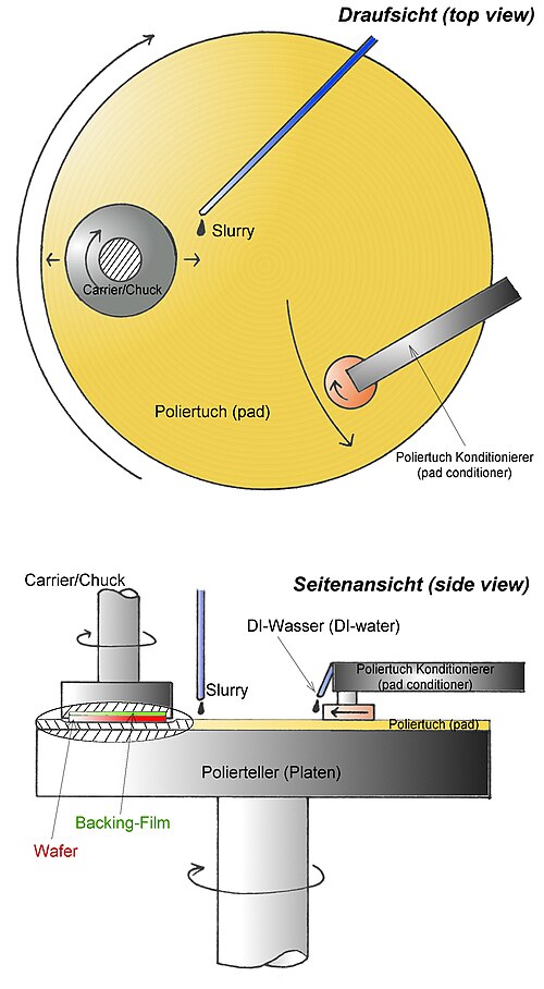
右側に示すような一般的なCMPツールは、パッドで覆われた非常に平坦なプレートを回転させる構造になっています。研磨されるウェーハは、裏打ちフィルム上のキャリア/スピンドルに上下逆さまに取り付けられます。保持リング(図1)は、ウェーハを正しい水平位置に保持します。ウェーハをツールにロードおよびアンロードするプロセス中、ウェーハはキャリアによって真空で保持され、ウェーハ表面に不要な粒子が付着するのを防ぎます。スラリー導入機構は、図1のスラリー供給部で示されるように、パッド上にスラリーを塗布します。プレートとキャリアの両方が回転し、キャリアは振動し続けます。これは、図2の上面図でよりよく確認できます。キャリアには下向きの圧力/下向きの力が加えられ、パッドに押し付けられます。通常、下向きの力は平均的な力ですが、除去機構には局所的な圧力が必要です。下向きの力は接触面積に依存し、接触面積はウェーハとパッドの両方の構造に依存します。通常、パッドの粗さは50μmです 。接触は突起部(通常はウェーハの高くなった部分)によって行われるため、接触面積はウェーハ面積のごく一部に過ぎません。CMPでは、ウェーハ自体の機械的特性も考慮する必要があります。ウェーハがわずかに反っている場合、中央部よりも端部の方が圧力が大きくなり、研磨が不均一になります。ウェーハの反りを補正するために、ウェーハの裏面に圧力を加えることで、中央部と端部の差を均一化できます。CMP装置で使用されるパッドは、ウェーハ表面を均一に研磨するために剛性が必要です。ただし、これらの剛性パッドは常にウェーハと位置合わせしておく必要があります。そのため、実際のパッドは、ウェーハの形状にある程度適合する軟質材料と硬質材料の積層体であることが多いです。一般的に、これらのパッドは30~50μmの細孔径を持つ多孔質ポリマー材料で作られており 、プロセス中に消耗するため、定期的に再調整する必要があります。ほとんどの場合、パッドは完全に独自規格であり、化学的性質やその他の特性ではなく、商標名で呼ばれるのが一般的です。
化学機械研磨(ケミカルメカニカルポリッシング)とは、化学的力と機械的力を組み合わせて表面を平滑化するプロセスです。化学エッチングと遊離研磨を組み合わせたハイブリッドな方法と考えることができます。
1990年頃までは、CMPは研磨によって粒子が発生しやすく、研磨剤自体にも不純物が含まれているため、高精度製造プロセスに組み込むには「汚れが多すぎる」と考えられていました。それ以降、集積回路業界はアルミニウム導体から銅導体へと移行しました。これにより、CMPの持つ、平面かつ均一な方法で材料を除去し、銅と酸化物絶縁層の界面で繰り返し停止できるという独自の能力を利用した、付加的なパターニングプロセスの開発が必要となりました(詳細は銅配線を参照)。このプロセスの採用により、CMP処理ははるかに広く普及しました。アルミニウムと銅に加えて、タングステンや二酸化ケイ素の研磨にもCMPプロセスが開発されています。
現在、CMPには研磨工程中に発生するいくつかの制約があり、新しい技術の最適化が必要とされています。特に、ウェーハ計測の改善が求められています[ 4 ]。さらに、CMPプロセスには、応力亀裂、弱い界面での剥離、スラリー化学物質による腐食攻撃など、いくつかの潜在的な欠陥があることがわかっています。今日の業界で最も古く、最も広く使用されている酸化膜研磨プロセスには、1つの問題があります。終点がないため、ブラインド研磨が必要となり、必要な量の材料が除去されたか、必要な平坦度が得られたかを判断するのが困難です。このプロセス中に酸化膜が十分に薄くならなかった場合、および/または必要な平坦度が達成されなかった場合、(理論的には)ウェーハを再研磨できますが、実際には生産において魅力的ではなく、可能な限り避けるべきです。酸化膜の厚さが薄すぎるか不均一すぎる場合は、ウェーハを再加工する必要がありますが、これはさらに魅力的ではなく、失敗する可能性が高いプロセスです。明らかに、この方法は時間とコストがかかる。なぜなら、技術者はこの作業を行う際に、より注意深く作業する必要があるからだ。
Shallow trench isolation (STI), a process used to fabricate semiconductor devices, is a technique used to enhance the isolation between devices and active areas. Moreover, STI has a higher degree of planarity making it essential in photolithographic applications, depth of focus budget by decreasing minimum line width. To planarize shallow trenches, a common method should be used such as the combination of resist etching-back (REB) and chemical mechanical polishing (CMP). This process comes in a sequence pattern as follows. First, the isolation trench pattern is transferred to the silicon wafer. Oxide is deposited on the wafer in the shape of trenches. A photo mask, composed of silicon nitride, is patterned on the top of this sacrificial oxide. A second layer is added to the wafer to create a planar surface. After that, the silicon is thermally oxidized, so the oxide grows in regions where there is no Si3N4 and the growth is between 0.5 and 1.0 μm thick. Since the oxidizing species such as water or oxygen are unable to diffuse through the mask, the nitride prevents the oxidation. Next, the etching process is used to etch the wafer and leave a small amount of oxide in the active areas. In the end, CMP is used to polish the SiO2 overburden with an oxide on the active area.
Key manufacturers and suppliers in the field of CMP include equipment vendors such as Applied Materials and Ebara Corporation. Suppliers of consumable polishing pads and slurries include Entegris, Qnity Electronics, Merck, Fujifilm, Hitachi, 3M, and Resonac.